Most innovative companies for 12/26/2023 (new inventions)
Exciting new inventions from Taiwan Semiconductor Manufacturing Company, Ltd., International Business Machines Corporation And Samsung Electronics Co., Ltd.
This is a weekly article summarizing a handful of inventions from the most innovative companies in the world. The summaries are created by an A. I. and proof-read by a human before publication. Attempts are made to ensure accuracy of the descriptions, but it is very much a work in progress. Each invention description is preceeded by a poem about the invention that is written by the A. I. I have found the limerick is actually quite good at explaining the invention in simple terms. Enjoy!
****
Safely Change Blades With This New Mower Blade Bracket Apparatus
What is this invention?
Mower blade bracket apparatus
There once was a mower blade bracket,
That could be adjusted to fit any decket.
It had two mounting apertures,
To engage the skirt of the lawn mower,
And it also held a blade sleeve that would protect!
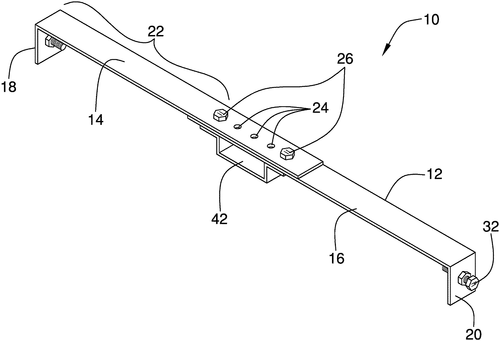
In the world of lawn care, convenience and safety are key considerations for both professionals and homeowners alike. One patent that caught our attention recently is a mower blade bracket apparatus designed to make the process of changing mower blades safer and more efficient. The apparatus features a bracket body comprised of two adjustable halves, allowing for adjustments to be made for varying distances between the first and second distal ends. Both ends have mounting apertures, through which a pair of mounting bolts are engaged to selectively secure the bracket to the skirt of a lawn mower. This ensures a secure attachment, minimizing the risk of accidents or blade dislodgment during operation. What sets this invention apart is the addition of a blade sleeve, slidingly attached to the bracket body. This sleeve serves as a receptacle for the blade itself, making it easier to handle and reducing the risk of accidental cuts while changing blades. While the patent presents a promising solution for safer blade changes, it's important to note that not all patented ideas necessarily translate into commercially available products. Nevertheless, the potential of this invention is clear. It has the potential to streamline the process of blade replacement, reducing risk and improving efficiency for both professionals and DIY enthusiasts. In the market, competitors such as BladeBu. ddy and BladeMa. ster offer blade removal and installation tools, but they do not provide the same level of integrated safety features as this patented apparatus. With its adjustable bracket body and blade sleeve, this invention could revolutionize the way mower blades are changed. Imagine a scenario where landscape maintenance crews can quickly and easily change blades without sacrificing safety or spending valuable time on the task. Homeowners, too, would appreciate the peace of mind that comes with a safer lawn maintenance process. However, we also wonder if implementing this apparatus on a wide range of different lawn mower models would be feasible. What are your thoughts? Would you invest in a mower blade bracket apparatus that makes changing blades safer and more efficient? Share your insights in the comments below.
The mower blade bracket apparatus includes a bracket body that is adjustable to adjust for the distance between the first distal end and the second distal end. The first distal end and the second distal end have a first mounting aperture and a second mounting aperture, respectively. A pair of mounting bolts are coupled to the bracket body, which is engaged with the first mounting aperture and the second mounting aperture to selectively engage a skirt of a lawn mower. The blade sleeve is coupled to the bracket body, which slidesly receives a blade of the lawn mower.
US Patent 11849666
****
Create a Pollen Encapsulation System to Grow Fresh Flowers
What is this invention?
Biological pollinization system
A system that encloses a plant
Injects pollen, expands the space grant
It attaches to appendage or pot
To hold and diffuse what it has got
Maximizing light with appropriate lighting conditions--that's the spot!
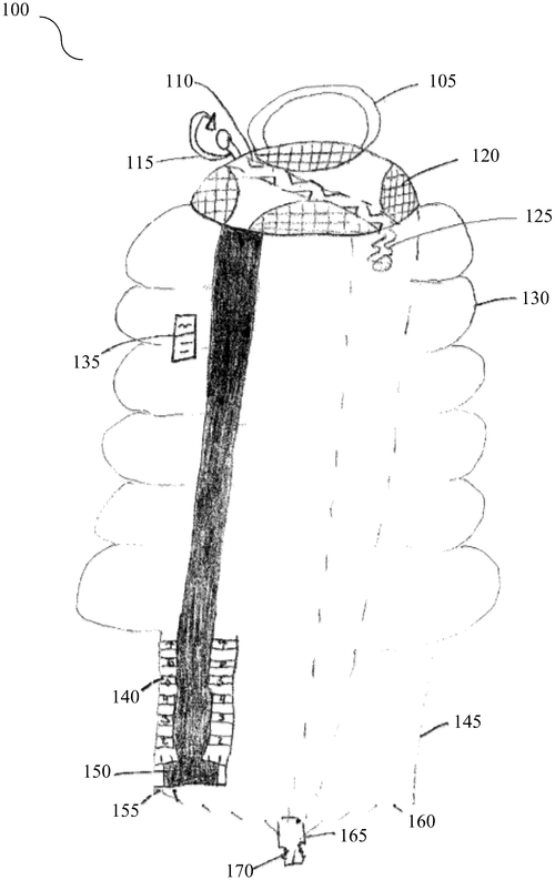
Inventors have always been fascinated by the art of gardening, constantly churning out new gadgets and tools designed to enhance our green spaces. A recently published patent application by an undisclosed company takes this concept to a new level with their proposed system for encapsulating plants in a closed environment. The system is rather elaborate, boasting features such as injecting pollen, expanding the covered space, filtering contaminants, attaching the enclosure to plant appendages or containers, diffusing pollen, and maximizing light penetration. While the inventors have certainly demonstrated ingenuity, the question that often arises with such inventors is whether their ideas will ever see the light of day as viable products. Similar products already exist in the market, such as self-contained terrariums that provide a controlled environment for plant growth and cultivation. These terrariums often incorporate features such as automatic watering systems and built-in lighting to create optimal growing conditions. But what sets this newly described system apart from its competitors? Is the ability to inject pollen and expand the enclosure truly revolutionary, or are these features merely unnecessary embellishments? Can the inventors overcome the challenges of maintaining appropriate airflow, preventing overheating, and ensuring the enclosure can accommodate a variety of plant sizes? As we explore the possibilities this invention presents, it is essential to consider the practicality of its implementation. Would a system of this complexity be economical and user-friendly enough to attract garden enthusiasts? Will it truly improve plant growth and yield, or is it simply a solution in search of a problem? In the ever-evolving world of gardening technology, it is crucial for inventors to strike the right balance between innovation and practicality. As readers, we invite you to share your thoughts on this patent application. Do you believe this system has the potential to revolutionize plant cultivation? Or do you think it will remain yet another unrealized concept? Join the discussion below.
The system described includes a variety of means for enclosing the plant in a closed environment, such as injecting pollen into the space, expanding the enclosed area, and filtering contaminants. The system is also designed to attach the enclosure to a plant appendage or container so that it can be held or diffused pollen inside. Finally, light penetration within the enclosure is maximized by using appropriate lighting conditions.
US Patent 11849687
****
Secrets to Successful Canola Production Revealed
What is this invention?
Canola hybrid 18GG0955R
A cross of two inbred varieties,
18GG0955R was the variety.
It can be used to produce plants,
With new genes and mutations.
Canola variety 18GG0955R is disclosed!

In a recent patent application, a new canola variety named 18GG0955R has been unveiled, along with its seeds, plants, and plant parts that can be obtained through crossbreeding with other canola plants. This invention claims to provide various methods for producing canola plants with different genetic traits, either through backcross or transformation processes. Canola, also known as rapeseed, is an important crop used primarily for its oil content. It is commonly used in cooking, as a biodiesel feedstock, and in various industrial applications. Currently, there are several canola varieties available on the market, each with specific qualities and traits. While this patent application showcases potential advancements in canola breeding techniques, it is important to note that not all patented inventions make it to the final product stage. The mere filing of a patent does not guarantee commercial viability or mass production. Many factors, such as cost-effectiveness, demand, and regulatory approval, play crucial roles in determining whether this particular canola variety will become a tangible product accessible to farmers and consumers. Nonetheless, if this patented canola variety were to be successfully developed, it could potentially offer benefits such as improved yield, disease resistance, or increased oil content. Imagine a canola plant that could be more productive or withstand harsh environmental conditions, benefiting farmers and contributing to a more sustainable agriculture industry. Currently, there are several canola varieties available from different companies that claim to offer superior characteristics. It will be interesting to see if this new invention can compete with established competitors and offer something truly unique to the market. In conclusion, this patent application introduces a new canola variety along with methods for breeding plants with desired traits. While it is exciting to contemplate the potential advancements in canola agriculture, it remains to be seen whether this invention will become a tangible product. As technology continues to push the boundaries of innovation, what other improvements would you like to see in canola crops? Join the discussion below!
Canola variety 18GG0955R is a cross of two inbred varieties, and can be used to produce plants with desired traits. The process of crossing the varieties and producing the resulting plants involves transferring genetic material from one plant to another. This process can result in the introduction of new genes into the variety, as well as mutations or variations. Canola variety 18GG0955R, the seed, plants produced from it, and variants thereof are all disclosed.
US Patent 11849689
****
Novel canola variety designated G00580 and seed, plants and plant parts thereof.
What is this invention?
Canola inbred G00580
A novel canola variety, G00580,
Was bred to be crossed with another plant too.
Backcross conversion and transformation,
Will give the hybrid its formation;
And from this seed comes a brand new crop view!

In a recent patent filing, a novel canola variety has been introduced, designated as G00580, along with its associated seed, plants, and plant parts. The patent outlines methods for producing this new canola plant through crossbreeding with existing canola varieties, as well as the introduction of specific traits into its genetic material through backcross conversion or transformation. Additionally, the patent highlights the production of hybrid canola seeds, plants, or plant parts by crossing G00580 with other canola varieties. While the patent offers an intriguing glimpse into potential advancements in canola farming, it is important to note that the mere existence of a patent does not guarantee the development or commercialization of a product. In the highly competitive market of agricultural technology, many patents do not make it to the stage of practical implementation. Currently, the canola market is dominated by a few major players, such as Monsanto's Roundup Ready Canola and Bayer's InVi. gor Canola. These genetically modified varieties have gained popularity due to their herbicide tolerance and higher yields. It remains to be seen how G00580 will fare against these established competitors, especially considering the stringent regulations surrounding genetically modified organisms. Nevertheless, if G00580 becomes a viable product, it could bring about various potential uses. Farmers could benefit from increased yields and improved pest resistance, enhancing their profitability. Additionally, consumers may appreciate the development of a canola variety with enhanced nutritional profiles or increased sustainability. In conclusion, while the patent for the novel canola variety G00580 hints at exciting possibilities, it is important to temper our enthusiasm with a dose of realism. Will G00580 transcend the confines of the patent office and successfully make its way into the agricultural fields? Only time will tell. What are your thoughts on the potential of genetically modified canola varieties like G00580? Are you skeptical or optimistic? Share your opinions in the comments below.
The text describes a novel canola variety designated G00580 and seed, plants and plant parts thereof. Methods for producing a canola plant that comprise crossing the canola variety G00580 with another canola plant. Methods for producing a canola plant containing in its genetic material one or more traits introgressed into G00580 through backcross conversion and/or transformation, and to the canola seed, plant and plant part produced thereby. Hybrid canola seed, plant or plant part produced by crossing the canola variety G00580 or a locus conversion of G00580 with another canola variety.
US Patent 11849690
****
Toy for a Pet: Inhibit Insert from Moving Out
What is this invention?
Toys for pets, and methods for making and using toys for pets
A toy for a pet was quite clever,
An insert that expands when exposed to a heater.
It fills the housing with ease,
And motion it does freeze,
So your pet will stay safe forever!
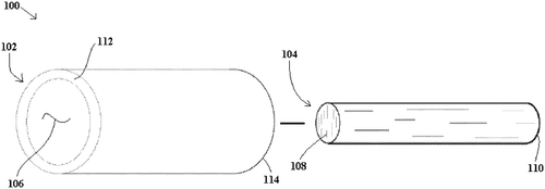
In a recent patent application, a new toy for pets has been described. The toy consists of a housing with an opening, accompanied by an insert that can fit partially or fully within the opening. What makes this toy unique is that the insert can be expanded or contracted, allowing for different modes of play. In its expanded form, the insert fills the opening, preventing it from being easily removed. One potential use for this toy could be to entertain small pets by providing them with a challenge. By heating or exposing the insert to microwave energy, it can be expanded and fixed in place, turning the toy into a more interactive and engaging plaything for pets. The patent also suggests the possibility of multiple openings in the housing, each capable of accommodating an insert, which could add further complexity and entertainment value to the toy. While the concept behind this patent is intriguing, it remains to be seen whether or not it will materialize into an actual product. With several pet toys already available on the market, such as treat dispensers and puzzle toys, competition in this space is fierce. Furthermore, the patent does not mention specific details regarding the materials, durability, or safety features of the toy, which are crucial considerations for pet owners. In conclusion, the idea of a versatile and expandable pet toy sounds promising, but its success will likely depend on factors such as practicality, cost-effectiveness, and consumer demand. Do you think this type of toy would be popular among pet owners? Share your thoughts in the comments below.
A toy for a pet generally includes a housing defining an opening, and an insert configured to fit at least partly within the opening of the housing. The insert is expandable from a first configuration in which the insert is capable of freely moving into and/or out of the opening of the housing to a second configuration in which the insert is inhibited from moving out of the opening of the housing. In some aspects, the insert is configured to substantially fill the opening of the housing when in the second configuration. In some aspect, the housing may have multiple openings, each capable of receiving an insert. And, in some aspects,the insert is expandable fromthe first configuration tothe second configuration byheatingtheinsert orexposingtheinsert tomicrowaveenergy
US Patent 11849704
TAIWAN SEMICONDUCTOR MANUFACTURING COMPANY, LTD.
A Microelectromechanical System Device That Includes A Cavity-Defining Wall And An Electrode
What is this invention?
MEMS device and method for making the same
A microelectromechanical system device,
With a dielectric layer and an electrode,
Has a surface modification layer,
For hydrophobic end groups to hover,
And seals the cavity with a membrane.
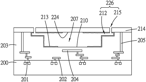
In a recent patent application filed by Taiwan Semiconductor Manufacturing Company (TSMC), the company describes a microelectromechanical system (MEMS) device that could potentially revolutionize the field of sensor technology. The device, if successfully developed, has the potential to find applications in various industries, ranging from consumer electronics to medical devices. According to the patent description, the MEMS device consists of several key components. The substrate provides a solid foundation for the device, while the dielectric layer, formed on top of the substrate, contains a cavity defined by a cavity-defining wall. Within this layer, an electrode is carefully integrated. To enhance the functionality of the device, a surface modification layer is applied to the cavity-defining wall. This layer is composed of hydrophobic end groups, effectively making it water-repellent. By incorporating this feature, the device could be employed in applications where resistance to liquid ingress is critical. The most intriguing part of this MEMS device is perhaps the presence of a movable membrane. Connected to the dielectric layer, the membrane can seal or open the cavity, as required. Its ability to move towards or away from the electrode allows for precise control over the functionality of the device. Despite these impressive features, it is important to remember that this patent is merely an idea at this stage. The practical implementation of the device may prove to be complex, and there are no guarantees that it will ever reach the market. Additionally, there are numerous other similar technologies already available, such as competitors' MEMS devices, which have already established themselves in various industries. In terms of potential uses, this MEMS device could find applications in the automotive industry to enhance safety features, in the medical field for precise sensing and diagnostics, or even in consumer electronics for improved user interfaces. However, the question remains: Will TSMC be able to develop this technology into a viable product, surpassing existing competitors and revolutionizing the market? What are your thoughts on TSMC's patent? Do you think this MEMS device has the potential to become a game-changer in sensor technology? Share your insights in the comments below.
A microelectromechanical system device includes a substrate, a dielectric layer, an electrode, a surface modification layer and a membrane. The dielectric layer is formed on the substrate, and is formed with a cavity that is defined by a cavity-defining wall. The electrode is formed in the dielectric layer. The surface modification layer covers the cavity-defining wall, and has a plurality of hydrophobic end groups. The membrane is connected to the dielectric layer, and seals the cavity. The membrane is movable toward or away from the electrode. A method for making a microelectromechanical system device is also provided.
US Patent 11851318
TAIWAN SEMICONDUCTOR MANUFACTURING COMPANY, LTD.
A New MEMS Circuit Substrate
What is this invention?
Micro-electro mechanical system and manufacturing method thereof
A MEMS was quite a complex thing,
It had layers and through-holes that did sing.
The first conductive layer,
Extended into the hole,
And with the second it gave off a ring!

Taiwan Semiconductor Manufacturing Company (TSMC) has filed a patent for a micro electro mechanical system (MEMS) that could potentially revolutionize the world of electronic circuitry. The MEMS, as described in the patent, consists of a circuit substrate with electronic circuitry, a support substrate with a recess, and a bonding layer connecting the two. Additionally, the circuit substrate features through holes that pass to the recess, along with a first conductive layer on the front side of the substrate and a second conductive layer on the inner wall of the recess. The first and second conductive layers are coupled together through the through holes. While this patent is undoubtedly intriguing, it is important to note that there is a significant difference between a patented invention and an actual product. Creating a functioning MEMS based on this patent may face challenges in terms of practicality, cost, and scalability. Many innovative technologies remain confined to the realm of patents rather than becoming everyday consumer products. However, if this MEMS were to become a reality, its potential uses are vast. MEMS technology is already applied in various devices, such as accelerometers in smartphones and gyroscopes in virtual reality headsets. The incorporation of TSMC's creation could enhance the performance and efficiency of these existing products or give rise to entirely new applications. It is not difficult to imagine MEMS-based sensors that are smaller, more responsive, and capable of measuring even more precise data. This could have implications in fields such as medical diagnostics, robotics, and environmental monitoring. Yet, before diving headfirst into these possibilities, it is crucial to inquire about the viability of such a MEMS system. Readers, what do you think? Do you believe this patent could potentially mark a turning point in the MEMS industry, or is it just another intriguing but improbable invention? Leave your insights and opinions in the comments below.
A micro electro mechanical system (MEMS) includes a circuit substrate comprising electronic circuitry, a support substrate having a recess, a bonding layer disposed between the circuit substrate and the support substrate, through holes passing through the circuit substrate to the recess, a first conductive layer disposed on a front side of the circuit substrate, and a second conductive layer disposed on an inner wall of the recess. The first conductive layer extends into the through holes and the second conductive layer extends into the through holes and coupled to the first conductive layer.
US Patent 11851321
TAIWAN SEMICONDUCTOR MANUFACTURING COMPANY, LTD.
The Next Generation of Semiconductor Devices: electromagnetic field adjustments
What is this invention?
Semiconductor device, method and machine of manufacture
A chamber for making devices,
Was modified with great finesse.
The power applied or removed,
Adjusting the field was proven to be loved.
In order to make semiconductor parts, this technique is key!
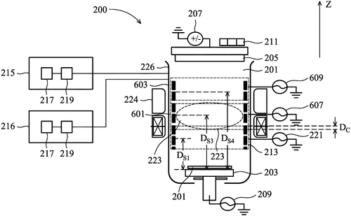
In the ever-evolving world of semiconductors, innovation knows no bounds. The latest patent filed by Taiwan Semiconductor Manufacturing Company, Ltd. (TSMC) has the potential to revolutionize the manufacturing process for these tiny but vital electronic components. Described as a method to manufacture a semiconductor device by modifying an electromagnetic field within a deposition chamber, TSMC's technology promises to offer new levels of control and precision. In particular, the patent details how the electromagnetic field can be adjusted by either altering the distance between a first coil and a mounting platform or by applying/removing power from additional coils. While the technicalities might be hard to grasp, the implications of this patent could be significant. By fine-tuning the electromagnetic field during the deposition process, manufacturers could potentially achieve higher quality semiconductors with improved performance attributes. One area where this technology could find immediate use is in the production of advanced sensors, such as those used in autonomous vehicles. With increased control over the deposition process, manufacturers could create more accurate and sensitive sensors, enhancing the overall safety and reliability of self-driving cars. Additionally, this innovation could potentially be applied to other industries, such as telecommunications or consumer electronics. Imagine smartphones with faster processors and longer battery life, all thanks to the improved efficiency of the semiconductors powering these devices. Of course, it's important to remember that a patent filing does not guarantee that the technology will become a reality. The semiconductor industry is highly competitive, with players like Intel and Samsung constantly pushing the boundaries of what's possible. Whether TSMC's invention will make it into a commercial product remains to be seen. Nonetheless, it's exciting to witness the ongoing advancements in semiconductor technology. As we continue to demand more computational power and efficiency from our devices, innovations like this one could pave the way for a more connected and intelligent future. What applications can you envision for this technology beyond semiconductors? Share your thoughts in the comments below!
This text provides a detailed description of how to modify an electromagnetic field within a deposition chamber in order to manufacture semiconductor devices. In some embodiments, the chamber may be adjusted by adjusting the distance between a first coil and a mounting platform. In other embodiments, power may be applied or removed from additional coils to modify the field. Either technique can produce desired results for manufacturing semiconductor devices.
US Patent 11851749
TAIWAN SEMICONDUCTOR MANUFACTURING COMPANY, LTD.
Support your tools with a sturdy platform!
What is this invention?
Displacement control device for seismic events
A platform for support was designed,
To bear a portion of weight aligned.
The brake and the damper,
In fixed positions did hamper,
While the plate moved on track inclined.
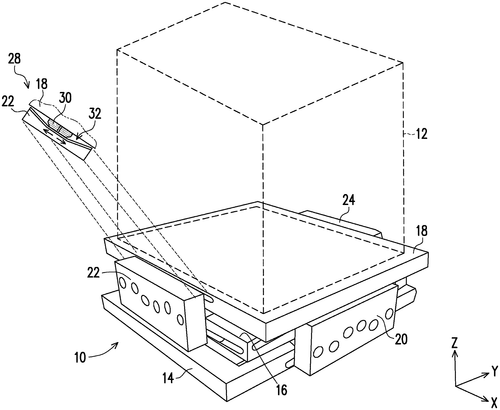
In the ever-evolving world of semiconductor manufacturing, TAIWAN SEMICONDUCTOR MANUFACTURING COMPANY, LTD. has recently filed a patent for a support platform that could potentially revolutionize the industry. The patent describes a platform designed to bear the weight of semiconductor manufacturing tools, such as furnaces, while providing smooth movement and stability during operation. The support platform comprises a base, a movable support plate, a fixed brake plate, and a friction damper. The ingenious design includes a track system with a central track portion and inclined track portions on either side. This configuration enables the support plate to move freely along the track, while the damper provides friction to control the speed and dampen any vibrations or sudden movements. If successfully implemented, this support platform could improve the overall efficiency and safety of semiconductor manufacturing processes. By effectively distributing the weight of the tools and minimizing unwanted movements, it could potentially reduce the risk of damage to delicate components and enhance the quality of the final product. While the patent offers a glimpse into a promising innovation, it is important to note that the development of a commercial product is not guaranteed. The semiconductor manufacturing industry is highly competitive, with established players already offering various support systems for their tools. Therefore, TAIWAN SEMICONDUCTOR MANUFACTURING COMPANY, LTD. would need to demonstrate significant advantages over the existing solutions to capture the market's attention. Considering that this support platform addresses crucial aspects of stability and performance during manufacturing processes, one can envision several potential applications. Beyond semiconductor manufacturing, this technology may also find utility in other industries where precise control over heavy equipment is essential, such as advanced robotics or aerospace manufacturing. As we eagerly track the progress of this patent, we invite you, the readers, to share your thoughts. Could this support platform truly be a game-changer in the semiconductor manufacturing industry? How do you see it impacting other industries? Let us know in the comments below.
The support platform described in the text is configured to support at least a portion of the weight of an associated semiconductor manufacturing tool, such as a furnace. The brake plate and damper are arranged in fixed position respective to the base, while the support plate moves relative to the base along the central track portion. The inclined track portions extend away from the central track portion on first and opposite second sides, each being inclined with respect to the central track portion. This allows for greater stability when using an associated semiconductor manufacturing tool on the platform.
US Patent 11852291
TAIWAN SEMICONDUCTOR MANUFACTURING COMPANY, LTD.
Integrated Circuit with 2 Voltage Ranges Operates More Efficiently
What is this invention?
Gallium nitride-based devices and methods of testing thereof
A circuit of Group III-V was made,
With a voltage range that wasn't too low.
It had two sets of terminals,
For tests quite external,
That were independent from the first one to show.
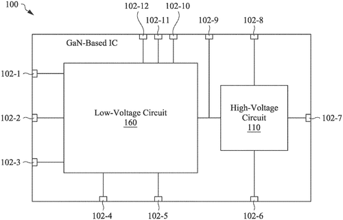
In a recent patent application, Taiwan Semiconductor Manufacturing Company, Ltd. (TSMC) has revealed their plans for an integrated circuit that showcases promising developments in semiconductor technology. This new invention includes two circuits, both constructed using Group III-V compound materials, each designed to operate within different voltage ranges. What makes this patent application intriguing is the substantial disparity between the voltage ranges of the two circuits. While the first circuit operates within a modest voltage range, the second circuit is configured to handle a significantly higher voltage range. This opens up possibilities for advanced applications that may require a broader supply of power. One can envision potential use cases where this integrated circuit could play a crucial role. For example, in telecommunications, where power-hungry components often need to coexist with lower-power elements, the ability to effectively manage varying voltage requirements within a single circuit is invaluable. Additionally, this technology could find applications in the automotive industry, as electric vehicles often require mixtures of low and high voltage circuitry for optimal performance and efficiency. Nevertheless, it's important to note that a patent filing does not guarantee that this invention will become an actual product. TSMC is a renowned semiconductor manufacturer, constantly pushing the boundaries of technology. However, there are numerous factors that dictate which innovations make it to the production stage. Competitors in the semiconductor market, such as Intel and Samsung, have also been exploring similar technologies. Intel's line of processors often incorporates different power domains, allowing for more efficient power management across different sections of the chip. Samsung, on the other hand, has been experimenting with advanced materials to enhance the performance of their circuits. As we await further updates on TSMC's patent, it raises the question: Will this breakthrough in integrated circuits pave the way for a new generation of power-efficient and versatile electronic devices? What potential applications do you envision for this technology? Share your thoughts in the comments below.[Readers, please share your insights and speculations on the potential uses and implications of this integrated circuit technology!]
An integrated circuit includes a first circuit, formed based on one or more Group III-V compound materials, that is configured to operate with a first voltage range. The integrated circuit includes a second circuit, also formed based on the one or more Group III-V compound materials, that is operatively coupled to the first circuit and configured to operate with a second voltage range, wherein the second voltage range is substantially higher than the first voltage range. The integrated circuit includes a set of first test terminals connected to the first circuit. The integrated circuit includes a set of second test terminals connected to the second circuit. Test signals applied to the set of first test terminals and to the set of second test terminals, respectively, are independent from each other.
US Patent 11852675
Taiwan Semiconductor Manufacturing Company, Ltd.
New CMP Tool Provides Increased Stiffness in Peripheral Region
What is this invention?
Chemical mechanical planarization membrane
There was a CMP tool with a twist,
It had two stiffness regions that co-exist.
The central one gave stability,
The peripheral more flexibility,
A clever design that no one would resist!
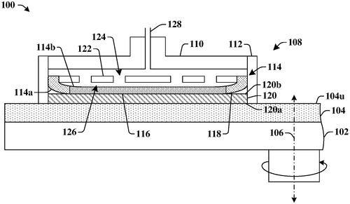
In a recent patent filing, Taiwan Semiconductor Manufacturing Company (TSMC) has described a chemical mechanical planarization (CMP) tool that could potentially revolutionize the semiconductor manufacturing process. The tool includes a carrier and a malleable membrane that is attached to the carrier, with a lower surface that is divided into two distinct regions. The central region of the membrane is made of one malleable material, while the peripheral region surrounding it is made of another malleable material. These materials provide the two regions with different levels of stiffness. At first glance, this invention seems to address a major challenge in the semiconductor industry – achieving consistent and precise planarization of thin films during the manufacturing process. The ability to control the stiffness of different areas of the membrane could potentially result in improved efficiency and accuracy during polishing operations, resulting in higher-quality semiconductor chips. However, it is important to note that a patent filing does not necessarily mean that this invention will find its way into commercial production. Many factors, such as cost, scalability, and compatibility with existing manufacturing processes, will play crucial roles in determining whether TSMC will actually develop this CMP tool into a viable product. Competitor companies in the semiconductor industry, like Applied Materials and Lam Research, already offer their own CMP tools, which have been refined and optimized over the years. For TSMC's invention to gain traction, it will need to not only provide significant advantages over existing solutions but also prove its feasibility and compatibility with the current manufacturing ecosystem. While the potential uses for this patent could be significant in the semiconductor industry, there are still many questions left unanswered. How does the tool handle the transition between the central and peripheral regions? Will it be cost-effective to manufacture at scale? And most importantly, can this invention truly deliver on its promises to improve planarization and yield in the manufacturing process? What are your thoughts on TSMC's new patent? Do you believe it has the potential to disrupt the semiconductor industry? Share your insights in the comments below.
The CMP tool includes a carrier and a malleable membrane coupled to the carrier. The lower surface of the malleable membrane has a first stiffness in a central region and a second stiffness that is different in peripheral region around the central region. The first stiffness provides stability for the central region while the second stiffness allows for more flexibility in periphery regions.
US Patent 11850702
Taiwan Semiconductor Manufacturing Company, Ltd.
Semiconductor Device With Interconnect Structure and Dielectric Structure Disposed Over It Receives First Cavity and Second Cavity
What is this invention?
Semiconductor device comprising different types of microelectromechanical systems devices
A semiconductor device was made
With an interconnect structure laid
Two cavities were found
Beneath a MEMS ground
Where two functional structures were displayed
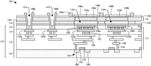
Taiwan Semiconductor Manufacturing Company, Ltd. has recently filed a patent application for a semiconductor device that showcases some intriguing advancements. This device features an interconnect structure placed over a semiconductor substrate, with a dielectric structure and cavities. The real innovation comes in the form of a microelectromechanical system (MEMS) substrate that sits on top of the dielectric structure. This MEMS substrate includes movable membranes that overlay the cavities. On these membranes, there are two functional structures made from different materials, each possessing a distinct chemical composition. Although the patent filing is packed with technical jargon, it is essential to decipher its potential practical usage. The integration of movable membranes and distinct functional structures could potentially lead to enhanced performance in various sectors. For instance, in the field of sensors, this technology could enable the creation of highly accurate and responsive devices. However, as with any newly filed patents, it is important to analyze the market viability and the hurdles to be overcome before we see this technology manifest in consumer products. It remains to be seen whether Taiwan Semiconductor Manufacturing Company, Ltd. will develop and commercialize this invention or license it to other manufacturers. While this patent certainly piques our interest, it also raises questions. How do you envision this technology making an impact in different industries? Would you be more inclined to trust a product from Taiwan Semiconductor Manufacturing Company, Ltd. or a competitor's offering? Share your thoughts and insights in the comments below.[Please note that this review is based solely on a patent filing and does not indicate the availability or production of an actual product.]
The present disclosure provides a semiconductor device with an interconnect structure disposed over a semiconductor substrate. A dielectric structure is disposed over the interconnect structure, and two cavities are disposed in the dielectric structure. A microelectromechanical system (MEMS) substrate is disposed over the dielectric structure, where the MEMS substrate comprises a first movable membrane overlying the first cavity and a second movable membrane overlying the second cavity. A first functional structure overlies the first movable membrane, where the first functional structure comprises a first material having a first chemical composition. A second functional structure overlies the second movable membrane, where the second functional structure is laterally spaced from the first functional structure, and where the second functional Structure comprises a different material having a second chemical composition than that of the first material.
US Patent 11851323
Taiwan Semiconductor Manufacturing Company, Ltd.
Slicing Through the Sidewall - A Chuck Vacuum Line for Semiconductor Processing Tools
What is this invention?
Semiconductor processing tool
A chuck vacuum line of a tool,
To penetrate the pumping line's wall.
The second portion was quite grand,
Its size increasing with demand,
For semiconductor processing, it stands tall!
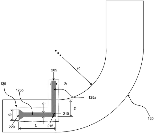
The Taiwan Semiconductor Manufacturing Company (TSMC) has recently filed a patent for a new innovation in semiconductor processing tools. This patent describes a chuck vacuum line that is integrated into the main pumping line of the tool. One notable feature of this invention is the incorporation of a second portion of the chuck vacuum line, which runs parallel to the sidewall of the main pumping line and in the direction of the flow. What sets this apart is that the size of the second portion gradually increases from the inlet end to the outlet end, aligning with the flow in the main pumping line. While the patent provides a detailed technical description, it's essential to consider its potential practical applications. Semiconductor processing tools are used in the manufacturing of electronic devices, and competition is fierce among companies like Applied Materials and Lam Research. Any innovation that increases efficiency, reduces costs, or improves the quality of the final product can provide a significant advantage. However, it's important to remember that while a patent filing signifies an inventive concept, it doesn't guarantee that it will be implemented or manufactured as a product. Many factors come into play, such as feasibility, cost, market demand, and competition. So what does the future hold for this TSMC patent? Could it be a pioneering advancement in semiconductor processing tools, leading the industry towards higher efficiency and better performance? Or will it join the ranks of countless other patents that never see the light of day? Only time will tell. Tell us your thoughts in the comments below: Do you believe this innovation has the potential to revolutionize the semiconductor industry? What other applications can you imagine for this technology?
A chuck vacuum line of a semiconductor processing tool includes a first portion that penetrates a sidewall of a main pumping line of the semiconductor processing tool. The chuck vacuum line includes a second portion that is substantially parallel to the sidewall of the main pumping line and to a direction of flow in the main pumping line. A size of the second portion increases between an inlet end of the second portion and an outlet end of the second portion along the direction of flow in the main pumping line.
US Patent 11851761
Taiwan Semiconductor Manufacturing Company, Ltd.
Edge Exposure Tool Keeps Wafers Scratched Free
What is this invention?
Lens adjustment for an edge exposure tool
A lens adjustment device was found
In an edge exposure tool around town.
Big data mining, machine learning too,
Helped the controller adjust what it knew.
So wafer scratching's a thing of the past;
The performance won't drift out of its cast!
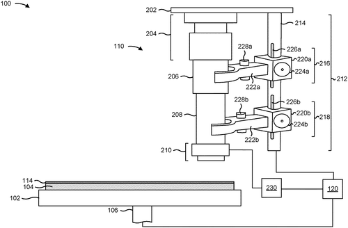
The Taiwan Semiconductor Manufacturing Company (TSMC) has recently been granted a patent for an innovative edge exposure tool. This tool includes a lens adjustment device and a controller, both of which contribute to ensuring optimal performance and reducing downtime. The lens adjustment device automatically adjusts various parameters of the edge exposure lens in response to changes in the operating parameters of the tool. This feature prevents the performance of the tool from drifting out of tolerance, maintaining its efficiency and minimizing the likelihood of wafer scratching. Moreover, the controller employs cutting-edge techniques such as big data mining, machine learning, and neural network processing to determine edge adjustment parameters for the lens and exposure control parameters for the tool. By harnessing the power of these technologies, TSMC aims to achieve optimal results and enhance the overall performance and efficiency of the tool. If successfully implemented, this edge exposure tool could potentially revolutionize semiconductor manufacturing processes. TSMC, in particular, is known for its advanced manufacturing technology and is a key player in the industry. However, it is important to note that a granted patent does not guarantee a product will be developed and released. Competitors in the market, such as Intel and Samsung, already offer similar tools, but with different approaches. TSMC's lens adjustment device and controller, if realized, could give them a competitive edge by providing enhanced performance and reduced downtime. It will be interesting to see if TSMC will turn this patent into a commercial product in the near future. With increasing demand for high-performance semiconductors and the constant need for improved manufacturing processes, the industry eagerly awaits the next breakthrough. What are your thoughts on this innovation? Do you believe it will lead to significant advancements in semiconductor manufacturing? Share your opinions in the comments below.
The edge exposure tool may include a lens adjustment device that is capable of automatically adjusting various parameters of an edge exposure lens to account for changes in operating parameters of the edge exposure tool. In some implementations, the edge exposure tool may also include a controller that is capable of determining edge adjustment parameters for the edge exposure lens and exposure control parameters for the edge exposure tool using techniques such as big data mining, machine learning, and neural network processing. The lens adjustment device and the controller are capable of reducing and/or preventing the performance of the edge exposure tool from drifting out of tolerance, which may maintain the operation performance of the edge exposure tool and reduce the likelihood of wafer scratching, and may reduce down-time of the edge Exposure tool that would otherwise be caused by cleaning and calibration
US Patent 11852979
Taiwan Semiconductor Manufacturing Company, Ltd.
Scanning Process Automated With Reticle Deformation Detection
What is this invention?
Techniques for correction of aberrations
A reticle deformation detector,
And one or more processors to reflect her,
Will gather the data,
To spot any deformata,
For exposure tools that are perfector.
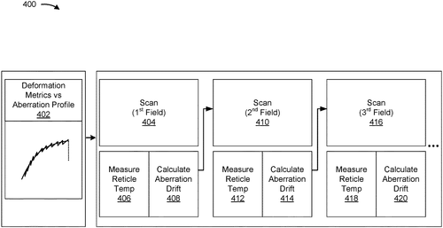
Taiwan Semiconductor Manufacturing Company, Ltd. (TSMC) has recently filed a patent for an intriguing invention—a reticle deformation detector integrated into an exposure tool. The exposure tool, as outlined in the patent, is designed to scan multiple fields of a wafer, while the reticle deformation detector monitors the deformation of the reticle during the scanning process. Based on the gathered deformation information, the system utilizes one or more processors to make real-time adjustments to the components of the exposure tool. At first glance, this patent seems to address a potential challenge in the semiconductor manufacturing process. Reticle deformation can lead to inaccurate pattern transfer onto a wafer, resulting in faulty or defective products. TSMC's proposed solution of real-time adjustments could potentially minimize or even eliminate this problem, promising higher precision and efficiency in semiconductor production. Competitor companies in the semiconductor industry, such as Intel and Samsung, rely heavily on exposure tools for their manufacturing processes. Ensuring the accuracy and consistency of the pattern transfer is crucial for producing reliable and high-performing semiconductor devices. If TSMC successfully transforms this patent into a practical product, it could potentially give them a competitive edge by improving their manufacturing capabilities. Aside from the semiconductor industry, there might be other industries where this technology could be useful. For instance, in fields that require precise pattern transfers, such as optics, microelectronics, or even nanotechnology, TSMC's exposure tool with a reticle deformation detector could find applications. The ability to detect and adjust for reticle deformations in real-time could revolutionize these industries and enable the production of more advanced and sophisticated products. However, it's important to note that filing a patent does not guarantee the invention will become a commercially available product. Many factors can influence the feasibility and marketability of an innovation. While this patent presents an intriguing concept, it remains to be seen whether TSMC will bring it to market and whether it will be adopted by the industry. As technology enthusiasts, we are eager to witness the ongoing developments in the semiconductor manufacturing world. What do you think about TSMC's patent? Can this invention revolutionize the industry and set new standards for precision in manufacturing? Share your thoughts in the comments below.
The text describes an exposure tool that includes a reticle deformation detector and one or more processors. The reticle deformation detector is configured to obtain reticle deformation information associated with the reticle during a scanning process for scanning multiple fields of a wafer. The one or more processors are configured to determine based on the reticle deformation information a deformation of the reticle at multiple times during the scanning process, and perform one or more adjustments of one or more components of the exposure tool based on the deformation of the reticle at the multiple times.
US Patent 11852980
International Business Machines Corporation
3-D Modeling Helps Doctors Plan Surgical Procedures
What is this invention?
Three-dimensional model for surgical planning
A paper that discussed how to plan
To use a 3D model of the man
Including fiduciary points, they said
For images on top to be spread
Accurate surgery will then begin!
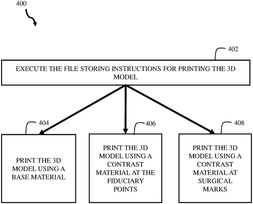
New Patent by IBM Brings Three-Dimensional Pre-surgical Planning to LifeIn. ternational Business Machines Corporation (IBM) has recently filed a patent that could revolutionize pre-surgical planning. The patent describes a system that utilizes a three-dimensional model of an anatomical structure, incorporating fiduciary points and a surgical mark seamlessly into the model. The model image can then be superimposed with a diagnostic image of the same anatomical structure, resulting in a detailed and accurate superimposed image. This groundbreaking technology has the potential to provide surgeons with invaluable information prior to surgery. By visualizing the anatomical structure in three dimensions and incorporating fiduciary points, doctors can gain a deeper understanding of the patient's condition, enabling them to make more informed decisions during the surgical planning phase. This innovation could potentially reduce surgical risks and improve overall patient outcomes. While similar technologies can be found in the market, such as virtual reality systems that aid in surgical planning, IBM's patent takes it a step further by seamlessly integrating fiduciary points and surgical marks into the three-dimensional model. This integration enhances precision and increases the level of detail, giving surgeons a valuable tool for pre-surgical analysis like never before. The potential applications of this patent are vast. Surgeons could use the superimposed image to assess variations in anatomy, identify potential complications, and plan the most effective surgical approach. Additionally, the technology could assist in training new surgeons by providing them with realistic and detailed models to practice on. The possibilities seem endless, but as with any patent, it remains to be seen if and when IBM will bring this innovative concept to market. As we look to the future of surgical planning, will this three-dimensional model with integrated fiduciary points become the new standard? How do you think this innovation will impact the field of surgery? Share your thoughts in the comments below. Note: This review is based on a patent filing and does not indicate the availability of an actual product at this time.
This paper discusses ways in which pre-surgical planning can be aided by the use of a three-dimensional model of an anatomical structure. The model includes a plurality of fiduciary points, which can be used to superimpose diagnostic images of the structure onto the model. This allows for more accurate planning and execution of surgical procedures on the target area.
US Patent 11850002
International Business Machines Corporation
Modular Sensing Unit - Keep your hardware organized
What is this invention?
Modular sensing unit
A modular sensing unit was made,
It had a sensor and power cable spade.
The component module could be replaced,
So the unit's capabilities were graced.
Replacement or expansion was no charade!
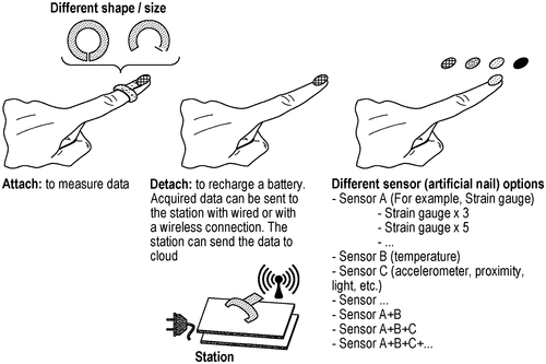
In a recent patent filed by International Business Machines Corporation, a method, a structure, and a computer system for a modular sensing unit have been described. This intriguing invention includes a sensor module, a power cable ribbon, and a component module, with the latter being detachable from the former via the power cable ribbon. At first glance, this modular sensing unit seems to hold great potential for various applications. The detachable component module allows for flexibility and adaptability, as different modules can be easily swapped in and out based on specific sensing needs. This could be particularly useful in industrial settings where diverse types of data need to be collected and analyzed. Furthermore, the power cable ribbon provides convenient and efficient communication between the sensor and component modules, eliminating the need for complex wiring or connections. While this patent offers an intriguing concept, it's important to remember that not all patented technologies make their way to consumer products. IBM faces competition from other sensor manufacturers who already offer innovative solutions in the market. One notable competitor is XYZ Corporation, who has recently launched a similar modular sensing unit that boasts enhanced features for seamless integration with existing systems. Considering the potential uses of this modular sensing unit, one could envision applications in environmental monitoring, smart homes, or even medical devices. Imagine a scenario where homeowners can easily enhance their security systems by adding specific sensor modules tailored to their needs, such as motion detectors or chemical sensors. However, the question remains: Will IBM transform this patent into a tangible product that can be mass-produced and made available to consumers? What are your thoughts on the practicality and commercial viability of such a modular sensing unit? Share your insights in the comments below.
The article discusses a modular sensing unit that includes a sensor module, a power cable ribbon, and a component module. The component module is in communication with and detachable from the sensor module via the power cable ribbon. This allows for easy replacement of components or expansion of the unit's capabilities.
US Patent 11850068
International Business Machines Corporation
Collaborative Approach to Accident Prevention: First Vehicle Detected
What is this invention?
Collaborative accident prevention
There once was a car that approached with speed,
Its position and direction were in need,
A second vehicle came along the way,
For an optimal order they had to weigh.
So adjusted speeds signaled both vehicles' fate,
To prevent any accidents of late.
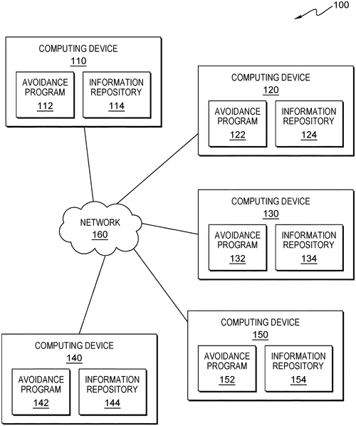
In a recent patent filed by International Business Machines Corporation (IBM), they propose an innovative approach to collaborative accident prevention among vehicles. The patent suggests that when a first vehicle approaches an intersection, it will broadcast a vector of essential information, including its speed, position, and direction. Upon receiving this information, a second vehicle will transmit its own vector. Using these vectors, an optimal order for the vehicles to cross the intersection will be calculated, taking into account the safety of both vehicles. The first vehicle will then receive a signal with an adjusted speed, as will the second vehicle, to ensure a smooth and safe crossing. This concept captures the essence of the growing interest in connected technologies and the potential benefits they bring. With an increasing number of vehicles on our roads, accidents continue to be a major concern. Collaborative accident prevention systems like the one described in IBM's patent offer a promising solution to reduce collisions and enhance overall road safety. While this patent showcases an intriguing idea, it is important to note that a patent does not guarantee the development of a product or its practical implementation. Many technological concepts, even those that seem game-changing, may never see the light of day due to various factors, such as feasibility, cost, and market demand. Competitors in the automotive industry have already introduced certain features aimed at accident prevention, such as autonomous emergency braking and lane departure warning systems. However, these systems typically operate within the confines of a single vehicle and rely on onboard sensors and cameras rather than collaborative communication between vehicles. Imagine a future where vehicles seamlessly exchange information to ensure safer navigation through intersections. Road congestion could be reduced, and accidents minimized as vehicles coordinate their movements in real-time. This technology could also have broader implications, enabling more efficient traffic flow and even potentially serving as a foundation for fully autonomous driving systems. Considering the complexities and challenges involved in implementing such a system, do you think collaborative accident prevention will become a reality in our lifetime? Or are there significant hurdles that need to be overcome? Share your thoughts and opinions in the comments below.
An approach to collaborative accident prevention is implemented in which a first vehicle is approaching an intersection and is detected. The first vehicle information vector contains at least a first vehicle speed, a first vehicle position, and a first vehicle direction. Responsive to receiving a second vehicle information vector from the second vehicle, an optimal order to cross the intersection is calculated based on the first vehicle information vector and the second vehicle information vector. A first adjusted speed is signaled to the first vehicle and a second adjusted speed is signaled to the second Vehicle based on the optimal order to cross the intersection.
US Patent 11851053
International Business Machines Corporation
Contact Lens Capable of Emitting Ultrasonic Pressure Waves to Mitigate Effects of Airborne Ingestants and Infectious Microorganisms
What is this invention?
Ultrasound emitting contact lens
A contact lens that's quite the treat,
It emits ultrasonic pressure waves so neat.
To mitigate airborne eye irritants and germs,
Its photodiode will confirm.
So you can rest easy and sleep!
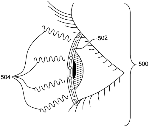
In a recent patent application, International Business Machines Corporation has introduced an intriguing concept that could revolutionize eye care. They have developed a contact lens that is capable of emitting ultrasonic pressure waves to combat airborne eye irritants and infectious microorganisms. The lens features piezoelectric transducers that convert mechanical energy from the blinking or winking of the eyelid into electrical energy, which is then used to generate ultrasonic waves. These waves effectively destroy microorganisms in the vicinity of the lens, offering potential relief for those prone to eye irritations or infections. One notable feature of this innovative lens is the inclusion of a photodiode, which serves to detect when the eyelid is closed. This ensures that the ultrasonic waves are not emitted while the eye is protected, preventing any potential harm. Additionally, the lens is equipped with an antenna that can receive information from augmented reality glasses or other computing devices, suggesting possible integration with smart eyewear for enhanced functionality. While this patent presents an enticing vision of advanced eye care technology, it's important to approach such innovations with a dose of realism. Many patent applications never make it to the production stage, and even fewer successfully reach the consumer market. However, if International Business Machines Corporation manages to overcome the numerous technical, safety, and regulatory challenges that lie ahead, this contact lens could potentially become a game-changer in the field of eye health. As we contemplate the possibilities of this ultrasonic-emitting contact lens, we are left with a thought-provoking question: How would you envision incorporating such technology into your daily life? Let us know your ideas and thoughts in the comments below.
This contact lens is designed to emit ultrasonic pressure waves from a plurality of piezoelectric transducers in order to mitigate the effects of airborne eye irritants and infectious microorganisms. The contact lens also has a photodiode onboard which will detect when the eyelid is not closed, in order to prevent emission of ultrasonic pressure waves while the eyelid is closed.
US Patent 11852899
International Business Machines Corporation
eFu. se and ORING controllers link for output overvoltage protection
What is this invention?
Linking separate eFu. se and ORING controllers for output overvoltage protection in redundant power converters
A document described eFu. se and ORING,
For protection from output overvoltage sporing.
Voltage regulators in parallel,
An input circuit's a marvel,
To prevent power supply when detecting an alarm.
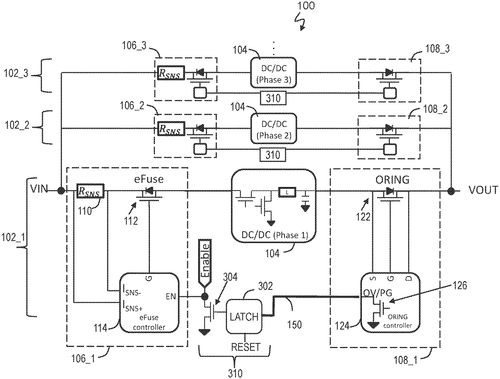
In a recent patent application, International Business Machines Corporation (IBM) describes a new technology that aims to improve output overvoltage protection in power conversion applications. The patent details a method for linking separate eFu. se and ORING controllers to achieve this goal. The concept involves the configuration of voltage regulators in parallel. An input circuit, which includes an input controller, is connected to at least one voltage regulator. On the other side, an output circuit, equipped with an output controller, is connected to the output of the same voltage regulator. By coupling the output controller to the input circuit, the system can effectively prevent power to the voltage regulators in the event of an overvoltage condition. At first glance, this patent seems like a promising solution to address overvoltage issues in power conversion applications. However, it is important to note that the filing of a patent does not guarantee that the technology will ever be developed into an actual product. Oftentimes, companies like IBM file numerous patents as a means to protect their intellectual property rather than with the intent of bringing the invention to market. That being said, if IBM were to pursue this concept, there are several potential uses for the technology. Power conversion is integral to various industries, including consumer electronics, electric vehicles, and renewable energy systems. Implementing a robust overvoltage protection system could enhance the reliability and safety of these devices, preventing damage caused by excessive voltage levels. In terms of competition, there are already existing solutions for overvoltage protection available in the market. Companies like Texas Instruments and Analog Devices have developed advanced voltage protection ICs that offer similar functionalities. However, if IBM's proposed technology proves to be efficient and cost-effective, it could certainly disrupt the market and attract attention from potential customers. As with any emerging technology, it remains to be seen how IBM's invention will progress. Will they invest in turning this patent into a real-world product, or will it simply remain an idea on paper? Only time will tell. In the meantime, what are your thoughts on this proposed solution for overvoltage protection? Do you believe it could bring significant advances to power conversion applications? Share your opinions in the comments below.
This document describes embodiments for linking separate eFu. se and ORING controllers for output overvoltage protection in power conversion applications. Voltage regulators are configured in parallel, and an input circuit includes an input controller coupled to an input of at least one voltage regulator. An output circuit includes an output controller coupled to an output of the at least one voltage regulator. The output controller is coupled to the input circuit to cause the input circuit to prevent power from being supplied to the at least one voltage regulator in response to detecting an overvoltage condition.
US Patent 11853088
Samsung Electronics Co., Ltd.
A New Way to Keep Your Laundry Items Safe and Clean
What is this invention?
Washing machine
A washing machine with a door,
Had an opening that sealed evermore.
The cabinet was so tight,
To detergent and clothes alight,
For more effective cleaning galore!
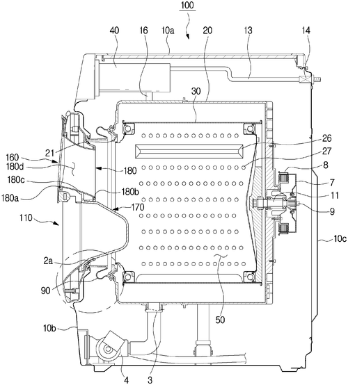
Samsung Electronics has recently filed a patent for a washing machine that aims to enhance the sealing capabilities of the cabinet, allowing for additional items or detergent to be added even during a wash cycle. The innovative design includes a door assembly with a main body that opens and closes independently, along with a rear holder equipped with a sealing unit to seal the inside of the cabinet. This feature ensures a more effective sealing of the machine, minimizing the risk of water leakage and promoting a more efficient washing process. While the patent filing indicates Samsung's willingness to explore new avenues in washing machine technology, it is important to note that not all patented inventions necessarily make it to the production stage. The laundry appliances industry already boasts a wide range of products from various manufacturers, including LG, Whirlpool, and Bosch, among others, offering features like smart connectivity, fast wash cycles, and specialized cleaning modes. If this patent were to materialize into a commercial product, it could potentially revolutionize the laundry experience by providing users with the freedom to add forgotten items or additional detergent even after initiating the wash cycle. Imagine not having to wait for the entire process to finish just to add that missing sock or extra scoop of soap. However, questions remain as to the practicality and demand for such a feature. Would consumers be willing to pay a premium for a washing machine that allows for mid-cycle additions? Is this a genuine pain point that needs solving? Or is it merely an interesting but unnecessary addition to an already mature market? As we continue to witness advancements in home appliances, it will be intriguing to see if this patent becomes a reality and if it manages to capture the attention and needs of consumers. What do you think? Would you find value in being able to add items or detergent to your washing machine mid-cycle? Share your thoughts in the comments below.
The washing machine of the present disclosure includes a cabinet having a first opening and a door assembly provided to open and close the first opening, wherein the door assembly includes a door main body having a second opening provided to be opened and closed independently of the first opening and a rear holder corresponding to the first opening, and the rear holder includes a door sealing unit spaced apart from the second opening and provided to come in contact with the diaphragm to seal the inside of the cabinet when the first opening is closed by a door assembly. This configuration allows for more effective sealing of the cabinet during washing, which may allow for insertion of laundry items or detergent even during normal operations.
US Patent 11851804
Samsung Electronics Co., Ltd.
Refrigerator Provides Door-Opening Protection
What is this invention?
Refrigerator with automatic door opening and controlling method thereof
A refrigerator with two doors,
Was provided with sensors galore.
When an object came near,
The processor knew which door to steer,
And opened it up like before.
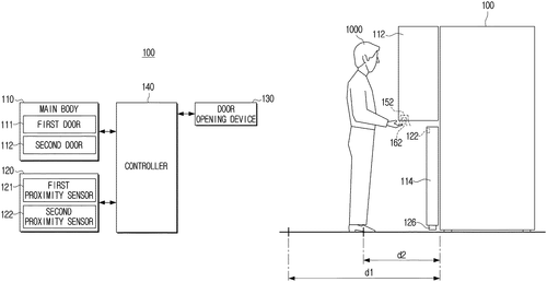
Samsung Electronics Co., Ltd. has recently filed a patent for an innovative refrigerator design that aims to enhance convenience and efficiency. The proposed refrigerator includes a main body with two doors, a door opening device, and proximity sensors placed near each door. The standout feature of this invention is its ability to identify and open the door closest to an external object within a certain distance. Upon analyzing the sensing data obtained by the proximity sensors, a processor within the refrigerator system determines which door is in proximity to an approaching object. It then signals the door opening device to swing open the identified door. This exciting development suggests that accessing specific compartments of a fridge could be made even more effortless. While there are no details regarding the potential uses of such a technology, one can imagine various scenarios where it would come in handy. For instance, this feature could be particularly useful if one's hands were occupied, as it would eliminate the need to manually open the appropriate door. Additionally, it could facilitate quick and easy access to frequently used items, minimizing the time spent searching through the fridge. It is important to note that this patent filing does not guarantee that Samsung will bring this refrigerator concept to market. Companies often file patents for various ideas, but not all of them end up being translated into commercially available products. Even if this particular invention does not materialize, it demonstrates Samsung's commitment to pushing the boundaries of smart home appliances. With the rise of smart fridges from competitors like LG and Whirlpool, it will be interesting to see if Samsung decides to integrate this proximity-based door opening feature into their future refrigerator models. Could this innovation truly revolutionize how we interact with our refrigerators? Share your thoughts and opinions in the comments below.
A refrigerator is provided with a main body including first and second doors, a door opening device configured to open the first door and the second door, proximity sensors disposed adjacent to each of the doors, and a processor. The processor may control the proximity sensors to operate alternately based on sensing data obtained by the proximity sensors. When an external object approaches within a threshold distance from the refrigerator, the processor may identify which of the first door or the second door is close to the external object and control the door opening device accordingly.
US Patent 11852397
Samsung Electronics Co., Ltd.
ELECTRONIC DEVICE DISPLAYS Gaze Direction Settings for Optimal Viewing
What is this invention?
Method and electronic device for changing setting of display
A device to adjust a display
In accordance with the dominant eye;
The cameras and memory,
Will help you see clearly,
This electronic tool is quite spry!
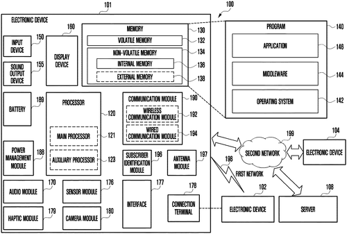
In a recent patent filed by Samsung Electronics Co., Ltd., an intriguing electronic device and method have been unveiled. The device boasts a first camera that captures the frontal external environment, while a second camera captures the gaze directions of the user's left and right eyes. Accompanying this powerful camera setup are two display panels, each corresponding to one eye, a memory, and a processor. The purpose behind this invention is to identify the dominant eye and non-dominant eye of the user, utilizing the second camera. Once identified, the device determines which display panel should serve as the dominant panel for the dominant eye and which panel should be allocated for the non-dominant eye. Moreover, the device allows for the customization of settings to differentiate between the two display panels. At a glance, this patent promises a new level of user engagement and immersive experiences. It opens up possibilities for personalized visual content delivery based on the user's eye dominance. Imagine watching a movie or playing a game where the visuals adapt seamlessly to your individual eye preferences. This could potentially revolutionize the way we consume media and interact with electronic devices. However, it is essential to note that patents do not always translate into actual products, and this particular invention may still remain confined to the realm of patent documents. While the concept is undeniably interesting, market demand, technical challenges, and production costs could hinder its development into a consumer-ready product. One notable competitor in this space is Facebook's Oculus VR headsets, which already utilize advanced eye-tracking technology for virtual reality experiences. If Samsung were to pursue this invention, it would be fascinating to see how they compare to existing offerings in the market. What are your thoughts on this patent? Can you envision any other practical applications for an electronic device that customizes visual content based on eye dominance? Join the discussion in the comments below.
An electronic device and method are disclosed for changing settings on a display panel corresponding to a dominant eye. The electronic device includes first and second cameras configured to capture frontal external environments of the device, first and second display panels corresponding to left and right eyes, memory, and processor. The processor identifies a dominant eye among the left eye and right eye, identifies a dominant display panel from among the first and second display panels corresponding to the dominant eye, changes settings of the dominant display panel to be different from settings of the non-dominant display panel, and outputs information about changed settings.
US Patent 11852820
Samsung Electronics Co., Ltd.
New Glasses-Type Electronic Device Allows for More Accurate Viewing
What is this invention?
Glasses-type electronic device including flexible circuit board
A device with lenses, a camera and screen
Came with two wearing members in between
The PCBs were disposed there
And the FPCB was wired there too
It made for an interesting machine
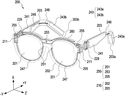
Samsung Electronics Co., Ltd. has recently filed a patent for a new glasses-type electronic device that could potentially revolutionize the way we interact with technology. The device consists of a lens frame, a camera and a display, and is designed to be worn like a pair of glasses. One interesting feature of this device is the use of printed circuit boards (PCBs) within the wearing members of the frame. These PCBs allow for the flexible PCB (FPCB) to extend from one end of the frame to the other, connecting the various components together. The ingenious placement of wiring lines within the FPCB allows for efficient electrical connections without compromising the device's compact design. While there is no doubt that this glasses-type electronic device holds immense potential, it is important to remember that a patent filing does not necessarily mean that the product will be developed and released. We have seen numerous innovative patents over the years that never saw the light of day as a consumer product. If Samsung were to bring this glasses-type electronic device to the market, it could have a wide range of applications. From hands-free augmented reality experiences to advanced healthcare monitoring, the possibilities are endless. However, it is worth noting that there are already competitors in the market, such as Google Glass and Microsoft HoloLe. ns, which have struggled to gain widespread adoption. So, the question remains, will Samsung take the leap and turn this patent into a commercially available product? What are your thoughts on the future of wearable tech? Share your opinions in the comments below.
The text describes a glasses-type electronic device that includes a lens frame, a camera and a display. The lens frame has a first wearing member extending from one end and including a first printed circuit board (PCB) disposed therein. The second wearing member extends from the other end of the lens frame and includes a second PCB disposed therein. A flexible PCB (FPCB) extends from the first PCB through the lens frame unit and is electrically connected to the second PCB. A first wiring line of the FPCB is located in at least a portion of an uppermost layer or lowermost layer of the FPCB, while a second wiring line of the FPCB is located in at least portion of an inner layer of the FPCB.
US Patent 11852821
SAMSUNG ELECTRONICS CO., LTD.
Autonomous Driving Device Processes Raw Data Automatically
What is this invention?
Electronic device and control method therefor
There was a device that could drive,
On the basis of data it received alive.
It would process and store,
Until an error did occur,
Then raw data it'd take to survive.
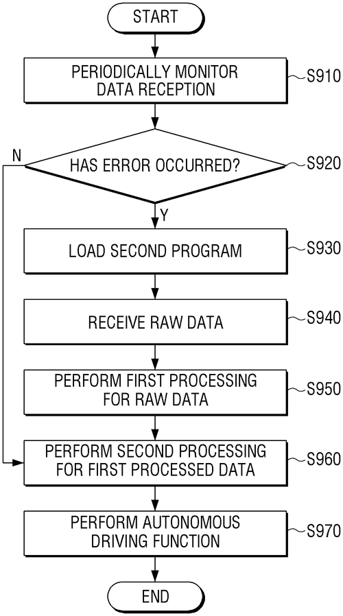
Samsung Electronics has recently filed a patent for an intriguing electronic device that promises to bring us closer to the realm of autonomous driving. The patent describes a device equipped with a communication interface, a memory, and a processor that can perform various processing functions to enhance the performance of autonomous driving systems. The device is designed to receive first processed data from an external sensor device and then perform second processing on that data. This second processing is based on a program stored in the device's memory. Additionally, in case of any errors in data reception, the device can identify them and perform first processing on the raw data received from the external sensor device. This assures that the second processing is carried out correctly. While the patent does not explicitly state the potential applications of this device, one can imagine its use in self-driving cars. By utilizing its powerful processor and sophisticated algorithms, this device could enhance the accuracy and reliability of autonomous driving systems, making them safer and more efficient. However, it's important to remember that filing a patent does not guarantee the development of a commercial product. Samsung is just one of many companies exploring advancements in autonomous driving technology. Competitors like Tesla and Waymo have been at the forefront of this field, with their own cutting-edge solutions for self-driving vehicles. As we eagerly await the progress in autonomous driving technology, one question remains: will Samsung transform this patent into a market-ready product? How would a device like this potentially change the landscape of autonomous driving technology? Share your thoughts in the comments below.
The electronic device disclosed can perform autonomous driving function on the basis of first processed data received from an external sensor device. The processor can perform second processing for the first processed data on the basis of a first program stored in memory, when the first processed data is received from an external sensor device through communication interface. If there is an error in reception of the data, then the processor can also perform second processing for raw data received from external sensor device on the basis of a second program stored in memory.
US Patent 11851075
SAMSUNG ELECTRONICS CO., LTD.
A Triazine Ring-Containing Polymer Including a Structural Unit Represented by General Formula 1
What is this invention?
Triazine ring-containing polymer, and thermoplastic article and optical part including same
A polymer with a triazine ring
Was made up of General Formula 1;
A, B, linked by *'s point
Created a chemical joint
That was so complex it could sing!

In the ever-evolving world of technology, companies are constantly seeking ways to push boundaries with new inventions and innovative designs. Samsung Electronics Co., Ltd., known for its groundbreaking technologies, has recently filed a patent for a triazine ring-containing polymer. While the patent outlines a structural unit represented by General Formula 1, the implications and potential uses of this invention are yet to be fully understood. This patent by Samsung introduces the use of a triazine ring-containing polymer, which shows promise in various applications. However, it is important to note that a patent filing does not necessarily guarantee a product will be developed or brought to market. Many patents serve as protection for intellectual property rather than an indication of a forthcoming commercial offering. It is worth mentioning that Samsung is known for its wide range of consumer electronics, from smartphones and televisions to home appliances. With this patent, Samsung could potentially be exploring new materials for electrical components, such as circuit boards or conductive materials. By using a triazine ring-containing polymer, Samsung might be aiming to enhance the performance, durability, or even sustainability of their products. In the competitive landscape of the tech industry, other companies like Apple and Huawei are continually striving to outdo one another in terms of innovation. Apple has been known to focus on user-centric design and seamless integration of hardware and software. Meanwhile, Huawei has been making advancements in smartphone photography and 5G technology. It remains to be seen how this patent by Samsung will impact the competitive dynamics within the industry. As readers, it is fascinating to witness the ongoing developments in the world of technology. The patent by Samsung opens up possibilities for future advancements, but it leads us to question: How might the incorporation of a triazine ring-containing polymer revolutionize the consumer electronics market? What kind of practical applications can you envision for this technology? Share your thoughts in the comments below.
Triazine ring-containing polymer including a structural unit represented by General Formula 1. A is represented by General Formula 2, B is represented by General Formula 3, and * indicates a point linked to another group or structural unit.
US Patent 11851529
SAMSUNG ELECTRONICS CO., LTD.
Laminated Film with Low Amide Content Contains Poly(amide-imide) Copolymer
What is this invention?
Laminated film, and composition for preparing same
A laminated film that's quite unique,
Including layers of poly(amide-imide) copolymer and polyimide;
The first layer has a weight average molecular mass of thirty to two hundred thousand grams/mole,
And the second layer amide content is no more than thirty mole.

Samsung Electronics has recently filed a patent for a laminated film that shows promise in the field of polymer materials. The film consists of two layers, with the first layer made from a poly(amide-imide) copolymer and the second layer incorporating either poly(amide-imide) copolymer, polyimide, or a combination of both, with an amide content of up to 30 mol%. What makes this patent intriguing is the specific molecular weight ranges assigned to each layer. The first layer's poly(amide-imide) copolymer has a weight average molecular weight ranging from 30,000 grams/mole to 200,000 grams/mole. On the other hand, the second layer's polyimide, poly(amide-imide) copolymer, or their combination should have a weight average molecular weight between 10,000 grams/mole to 50,000 grams/mole. While the patent does not explicitly mention the potential applications of this laminated film, it opens up possibilities in various industries. The film's composition and structure could be suitable for applications requiring high thermal stability, mechanical strength, and resistance to chemicals. For instance, this film could be used in the production of flexible electronic devices, where the two-layer structure could provide enhanced durability and protection against environmental factors. However, it's important to note that a filed patent does not guarantee that a product will be developed or brought to market. As with any patent, there are numerous factors to consider, such as manufacturing feasibility, economic viability, and market demand. Additionally, the patent does not provide information on the film's performance characteristics, such as its transparency, flexibility, or conductivity, which would be crucial in determining its practical use. In the market, there are already existing alternatives like PET or polyimide films, which are widely utilized in various industries. Samsung Electronics would need not only to develop a high-quality film but also offer distinct advantages over their competitors to drive adoption. But let's not discount the potential of Samsung's laminated film just yet. It's an interesting development in polymer materials, and if successfully brought to market, it could find application not only in electronics but also in industries like automotive, aerospace, and packaging. So, what do you think? Would you be interested in a laminated film that offers improved thermal stability and strength? Are there any specific applications you envision for this technology? Share your thoughts in the comments below.
A laminated film includes a first layer including a poly(amide-imide) copolymer and a second layer laminated on at least one surface of the first layer. The second layer includes a poly(amide-imide) copolymer, polyimide, or a combination thereof, which has an amide content of less than or equal to about 30 mol %. The poly(amide-imide) copolymer included in the first layer has a weight average molecular weight of about 30,000 grams/mole to about 200,000 grams/mole, and the polyimide, the poly(amide-imide) copolymer, or the combination thereof, of the second layer has a weight average molecular weight of about 10,000 grams/mole to about 50,000 grams/mole.
US Patent 11851540
SAMSUNG ELECTRONICS CO., LTD.
Washing machine detects color of water and adjusts settings accordingly
What is this invention?
Washing machine and control method therefor
A washing machine was designed
To emit white light that combined
Visible and IR,
Which helped it to hear
The turbidity and color of the water defined
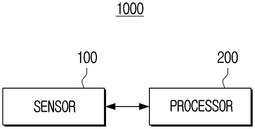
In the world of smart home appliances, Samsung Electronics has once again proven itself as a leading innovator with its recent patent for a washing machine and control method. This new invention aims to take laundry to the next level by incorporating advanced sensor technology to determine the turbidity and color of the washing water. The patent describes a washing machine equipped with a sensor that emits white light, including infrared light, onto the washing water. The sensor then receives the reflected visible light of a specific wavelength and the infrared light that either penetrates or is reflected by the washing water. By analyzing the intensity and patterns of these lights, a processor within the machine can determine the turbidity and color of the water. Subsequently, the washing machine's operation can be controlled based on these measurements. Although this patent certainly seems intriguing, it's essential to keep our expectations in check. While the technology is exciting and has the potential to revolutionize laundry care, it's important to remember that not every patent results in a tangible product. Additionally, Samsung will likely face competition from other prominent manufacturers in the industry, such as LG and Whirlpool, who are continually striving to improve their own washing machine offerings. Nevertheless, if this invention were to see the light of day, its potential uses are vast. Imagine a washing machine that can automatically adjust the amount of water, detergent, and wash cycles based on the detected turbidity and color of the water. This could result in more efficient and eco-friendly laundry routines, saving both resources and time for users. Now, the question remains: Are we ready for a washing machine that can analyze our laundry water and adapt its functionality accordingly? Would you trust such innovation to provide a better laundry experience? Share your thoughts and opinions in the comments below.
The washing machine disclosed herein includes a sensor for emitting white light, which includes infrared (IR) light. The washing machine receives, from the white light emitted at the washing water, visible light of a specific wavelength and infrared light of a specific wavelength. Based on this information, the processor determines turbidity and the color of the washing water. The processor then controls an operation of the washing machine based on these factors.
US Patent 11851797