Most innovative companies for 11/28/2023 (new inventions)
Exciting new inventions from International Business Machines Corporation, Micron Technology, Inc., Canon Kabushiki Kaisha And Apple Inc.
This is a weekly article summarizing a handful of inventions from the most innovative companies in the world. The summaries are created by an A. I. and proof-read by a human before publication. Attempts are made to ensure accuracy of the descriptions, but it is very much a work in progress. Each invention description is preceeded by a poem about the invention that is written by the A. I. I have found the limerick is actually quite good at explaining the invention in simple terms. Enjoy!
****
Instruments to Determine Level and Plumb Orientations Include Eye-catching Bubble Chambers
What is this invention?
Instrument for determining level or plumb orientations
A tool that can tell if an object is level or plumb,
It has a body with openings to see from the front and back.
Contained in each chamber are convex sides, some air, and fluid too,
So you can spot the bubbles from all directions around the view.

In today's world of precision measurements, determining level or plumb orientations has become essential in various industries, from construction to engineering. A recently issued patent showcases an instrument that aims to simplify this process, offering a potentially innovative solution to the age-old problem of ensuring accurate orientations. The instrument, described in the patent, consists of an elongated body equipped with multiple orientation measurement devices. Each device is capable of indicating either a level or plumb orientation, depending on the position of the instrument. The measurement devices comprise chambers with convex sides, containing a fluid and an air bubble that floats within. What makes this invention intriguing is the thoughtful design of the elongated body. It features two sets of openings: the first set accommodates the embedding of the orientation measurement devices, ensuring their secure placement within the instrument. Meanwhile, the second set of openings permits viewing of the bubbles from both the front and back of the elongated body, as well as from the top and bottom. The potential applications for such an instrument are vast, with usability ranging from everyday household tasks to professional construction sites. Imagine using it to hang a picture frame perfectly level or ensuring that a newly constructed building is plumb and aligned accurately. However, it is crucial to consider whether this patent will ever translate into an actual product. While the concept presented in the patent seems promising, we must acknowledge that the market is already saturated with various competitors offering similar solutions, such as digital levels and laser-based orientation tools. These existing technologies have gained popularity due to their precision and ease of use. Consequently, the patent holder of this instrument would need to offer compelling advantages to convince consumers to adopt their product over the competition. In conclusion, the patented instrument for determining level or plumb orientations certainly provides a fascinating idea and potential convenience for users. However, its success in the market remains uncertain, as it must contend with established competitors that have captured the trust of consumers. Time will tell whether this invention will make its way from patent to practical product. Now, we would love to hear from you, our readers. Are you intrigued by this instrument? Can you envision a specific scenario where it would be beneficial? Share your thoughts and opinions in the comments below.
This instrument can be used to determine whether an object is level or plumb. It includes a body with a set of openings that allow the orientation measurement devices to be seen from the front and back of the body. The devices each contain a chamber with convex sides, a fluid, and an air bubble. The bubbles are visible from all directions around the body.
US Patent 11828595
****
3D Roadway Cuboid Nodal System Detects Mobile Devices
What is this invention?
Controlling vehicles in a complex ecosystem
There was a system that assessed
The usage of roadway segments and nodes best
It had a computing device
That checked the mobile node's price
To make sure they were used with finesse
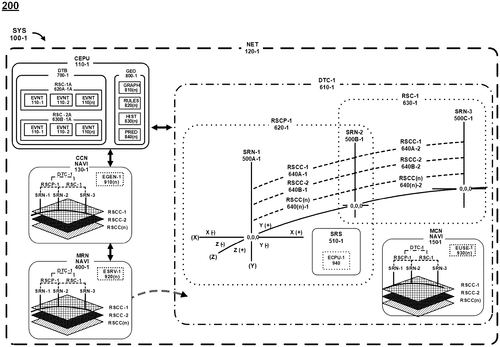
In the world of transportation technology, patents often give us a glimpse into the future of how we'll get from point A to point B. One recent patent that has grabbed attention is the "three-dimensional roadway segment cuboid nodal system and stationary resource node subsystem(s)." While the name may not roll off the tongue, the concept behind it is certainly intriguing. This patent describes a computing device that aims to acquire information about a mobile node (presumably a vehicle) and a three-dimensional roadway segment cuboid subsystem. It then uses this information to identify and determine acceptable usage. In simpler terms, it seeks to optimize traffic flow and resource allocation by effectively managing the movement of vehicles on three-dimensional roadways. If successfully implemented, this technology could have significant implications for transportation as a whole. Imagine a traffic system that dynamically adjusts the flow of vehicles based on real-time data, seamlessly guiding them through interconnected roadways and minimizing congestion. Additionally, the ability to allocate resources efficiently could lead to reduced fuel consumption and a greener, more sustainable transportation infrastructure. Of course, as with any patent, we must temper our enthusiasm with pragmatism. Turning a patent into a viable product is no small feat, and there are bound to be numerous hurdles along the way. Furthermore, competitors in the transportation sector have already introduced similar concepts, such as autonomous vehicles and smart city initiatives. The question then becomes, can this patent offer something unique and compelling enough to stand out from the crowd? Only time will tell if this three-dimensional roadway segment cuboid nodal system and stationary resource node subsystem(s) will make it from the filed patent to the reality of our streets. In the meantime, it's fascinating to see the innovative ideas that individuals and companies are envisioning to shape the future of transportation. So, what do you think? Could this patent revolutionize the way we travel, or is it just another ambitious vision that may never come to fruition? Let us know your thoughts in the comments below.
This text describes a system that allows for the assessment of acceptable usage of roadway segments and stationary resource nodes. The system includes a computing device that acquires information regarding a mobile node and the roadway segment cuboid subsystems associated with the mobile node. This information can be used to determine if the use of the roadway segment or stationary resource node is appropriate.
US Patent 11828608
****
A System for an Autonomous Vehicle by Providing Lane Markers
What is this invention?
Roadway information detection sensor device/system for autonomous vehicles
A system to help drivers on the go,
For navigation and safety in tow.
The lane markers they place,
Will send back a trace,
So you never have to guess where you'll go!
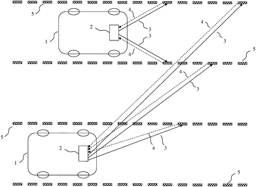
In a recent patent application, a new system was described that could potentially revolutionize the capabilities of autonomous vehicles. The patent outlines a method for improving road navigation by providing lane markers on the road that vehicles can read and use to navigate. Essentially, the idea is to transmit a discovery signal from the vehicle to the marker, which then returns information about the marker's position on the road and how the vehicle should proceed. This system has the potential to significantly enhance the accuracy and reliability of autonomous vehicles when it comes to real-time road navigation. Currently, many autonomous vehicles rely on a combination of sensors and sophisticated algorithms to interpret and understand their surroundings. However, this patent suggests that using physical lane markers in conjunction with an autonomous control system or a 3D map navigation database could eliminate the need for complex sensor technology. While the concept described in the patent is undoubtedly intriguing, it is important to note that this is still just a patent application. As with many patents, there is no guarantee that this invention will ever be brought to market. Additionally, it is worth considering existing competitor products in the autonomous vehicle space. Companies like Tesla, Waymo, and Uber are constantly pushing the boundaries of autonomous vehicle technology and may already have similar lane navigation systems in development. If this system becomes a reality, its potential uses could be far-reaching. Autonomous vehicles equipped with this technology could navigate complex road systems more effectively, potentially improving safety and efficiency. Furthermore, it could provide a reliable solution for autonomous vehicles in areas with poor connectivity or limited GPS signal. While we wait to see whether this patent will become a reality or remain merely an idea, we're curious to hear your thoughts. How do you envision a system like this being integrated into autonomous vehicles? Could it be a game-changer for the industry, or do you have reservations about its feasibility? Share your opinions in the comments below!
The system described in this paper is designed to help drivers navigate roads safely and efficiently. The lane markers are placed at strategic points on the road, and when a vehicle enters or leaves the marker, it will transmit a discovery signal back to the system. This information will then be used to determine the direction of the vehicle in real time, as well as its position on the road. Depending on which type of navigation system is being used, either an autonomous control system or 3D map navigation database may be used to provide this information.
US Patent 11828610
****
Get directions to your destination with ease!
What is this invention?
Method and apparatus for setting destination in navigation terminal
A method and an apparatus were found,
For displaying a route on the ground.
The message received from the second device,
Had location info to suffice.
From start to destination with ease, no more need for keys!
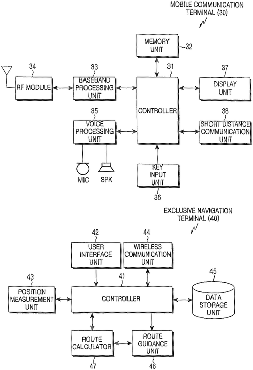
Innovative Patent Aims to Streamline Route Display on Electronic Devices. A newly discovered patent has caught the attention of technology enthusiasts, promising to revolutionize route display on electronic devices. The patent outlines a method and apparatus that would allow a first electronic device to display a route based on received information from a second electronic device. This could potentially spell good news for anyone who frequently uses mapping or navigation apps on their smartphones or tablets. The patent describes a process wherein a message is received from a second electronic device. By analyzing the contents of the message, the patent claims to identify location information including the address details that were inputted by the user of the second device. This information is then obtained and used in conjunction with the second location information of the first electronic device. Once the user sets their start location as the second device's location information and their destination as the selected address information, the method further involves obtaining route information between the two points. This route, which represents the obtained route information, is then displayed on the first electronic device's screen. Although the potential applications of this patent seem promising, it is important to note that having a patent does not necessarily mean a product will be developed from the idea. Many factors, such as market demand, technical feasibility, and competition from existing products, can influence the fate of patents. For avid travelers and frequent commuters, this technology could offer a more seamless experience in navigating unfamiliar routes. It could also potentially simplify the process for arranging meet-ups, saving time and effort in providing detailed directions. However, with competitors such as established navigation apps and smart devices already dominating the market, it remains to be seen whether this patent will ever see the light of day as a consumer product. What do you think? Would you find this route display method useful in your daily routine? Are there any specific scenarios where you can envision its potential benefits? Let us know in the comments below!
A method and an apparatus are provided for displaying a route in a first electronic device. The method includes receiving a message from a second electronic device. Based on analyzing the received message, first location information including address information inputted from the user of the second electronic device is identified. The first location information is obtained from the received message. Second location information of the first electronic device is obtained. A start location is set to the obtained second location information and the destination location is set to the selected address information. Based on obtaining route information between the start location and the destination location, a route representing the obtained route information between the start location and the destination location is displayed on a display of the first electronic device.
US Patent 11828612
****
Keep your data safe with this magnetic security system!
What is this invention?
Proximity sensing components employing enhanced security communications
A system was created with care,
To ensure that no one could enter there.
It had a first part,
That emitted an auth code start,
And then another to sense the magnetic field near!
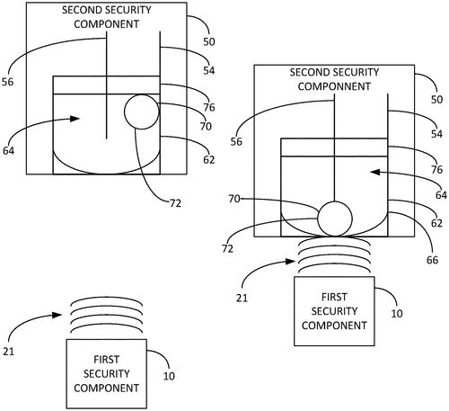
In the ever-evolving landscape of security technology, a recent patent application has caught the attention of industry insiders. The patent describes a system that aims to revolutionize wireless security by utilizing magnetic fields for authentication purposes. The system consists of two key components. The first is a security device equipped with a magnetic field generator. This device emits a signal containing an authorizing code, which is embedded within a magnetic field. The second component is a security device that can wirelessly receive this signal when it comes into proximity with the magnetic field. What sets this technology apart is its innovative use of magnetic fields for secure communication. By employing a magnetic field sensor, the receiving device can detect and interpret the signal emanating from the magnetic field generator. This sensor can also change between two states based on fluctuations in the signaling magnetic field. While the patent application provides an intriguing glimpse into the future of wireless security, several questions remain. Will this system be able to effectively compete with existing security solutions on the market, such as biometric authentication or encrypted wireless communication? What potential applications could arise from this technology beyond traditional security measures? As the development and implementation of this patent remains uncertain, it is undoubtedly an area to keep a close eye on. Will this technology become a reality, or will it simply remain an interesting concept? We invite you to share your thoughts and insights in the comments below.
A system may include a first security component that emits a signal with an authorizing code and a magnetic field generating device that generates a signaling magnetic field including the signal with the authorizing code. The second security component can receive the signal with the authoring code when it is proximate to the signaling magnetic field of the first security component. The second security component may have a magnetic field sensor that changes between first and second states based on whether or not there is a change in the signaling magnetic field.
US Patent 11828624
International Business Machines Corporation
Method Identifies Indoor Temperatures That Need to Be Modified
What is this invention?
Image analysis for temperature modification
There was a method for modifying the heat,
It started with images of those you'd meet.
The occupant's traits were identified and compared,
And if the discrepancy factor exceeded what was declared,
A modification to the first temperature could be initiated neat!
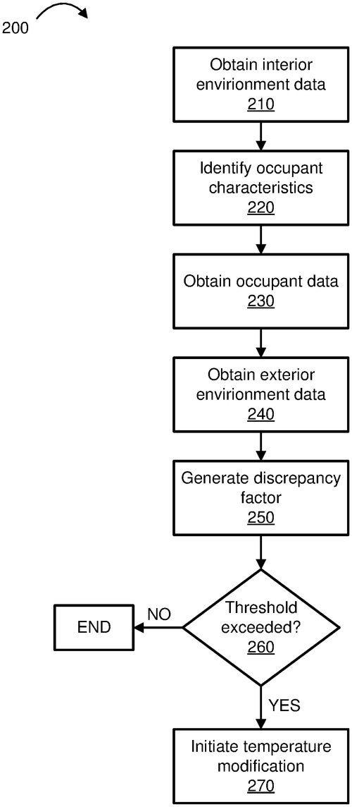
In a recently published patent application, International Business Machines Corporation (IBM) describes a method that aims to enhance the comfort levels of occupants in an interior environment. The patent suggests the use of a set of images to obtain information about the occupants and their corresponding characteristics. By comparing this information to the temperature of the external environment, IBM's method generates a discrepancy factor to determine if adjustments need to be made to the interior temperature. While this patent application introduces an interesting concept, it remains to be seen if it will evolve into a viable product. Competitors in the smart home and building automation industries have already released temperature control systems that rely on various sensors and algorithms to optimize comfort and energy consumption. As such, it is important to consider the potential benefits and drawbacks of this new approach. One potential use of IBM's method could be in commercial buildings, where the system could identify patterns in occupant behavior and adjust the temperature accordingly. This could lead to reduced energy expenses and increased occupant satisfaction. Additionally, in residential settings, such a system could adapt to the preferences of different family members, reducing the need for manual adjustments. However, it is essential to address potential privacy concerns that may arise from using occupant images to gather data. IBM would need to ensure strict security measures are in place to protect the privacy of individuals. Furthermore, the practicality and cost-effectiveness of implementing such a system on a large scale would need to be thoroughly evaluated. As with any emerging technology, the path from patent to product is a complex one. The mere existence of a patent application does not guarantee that a tangible product will follow. So, while IBM's method shows promise, it remains to be seen whether it will reach consumer markets. What are your thoughts on using occupant characteristics and external temperature to control interior environments? Do you believe this method has potential, or do you foresee any challenges in its implementation? Share your views in the comments below.
The text describes a method for modifying a temperature in an environment. The method can include obtaining a set of images of the occupants, identifying the occupant characteristics based on the set of images, and comparing the occupant characteristics to a second temperature. If it is determined that the discrepancy factor exceeds a threshold, then a modification to the first temperature can be initiated.
US Patent 11829166
International Business Machines Corporation
Disclosed embodiments provide techniques for generating and using a Global Error-Code Sequence (GECS)
What is this invention?
Globally unique error codes for knowledge document indexing in software systems
A document full of helpful advice,
To generate a unique error ID.
The GECS forms correlation strong,
So downtime it won't prolong,
And application problems will quickly subside!
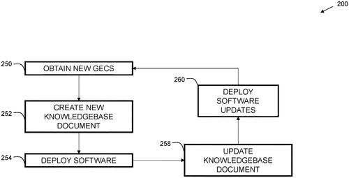
In a recent patent filing, International Business Machines Corporation (IBM) has introduced a promising technique that aims to revolutionize error identification and resolution in computer applications. The patent describes a system called the Global Error-Code Sequence (GECS), which generates unique error identification numbers (IDs) to help quickly diagnose and resolve software issues. Traditionally, error tracking mechanisms in software rely on various elements like line numbers, stack traces, and addresses. However, these can be prone to changing with new releases or invocations, making it challenging to establish a concrete link between an error and its solution. Here is where IBM's GECS steps in, providing a robust correlation between an error condition and a knowledgebase document, resulting in faster problem resolution and reduced downtime. The potential uses for this technology are vast. Imagine an eCo. mmerce application ecosystem utilizing the GECS, where errors can be pinpointed accurately, allowing developers to swiftly address issues and get the system back up and running without major disruptions. Similarly, on a larger scale, organizations worldwide can implement the GECS to streamline error resolution processes, minimizing their impact on productivity. While IBM's patent presents an intriguing solution to a common problem in software development, it must be noted that not all patented inventions translate to tangible products. The journey from patent filing to practical implementation can be a long and complex one, requiring significant investment and market demand. As excited as we may be about the potential benefits of the GECS, it remains to be seen if IBM will transform this concept into a real-world solution. In the realm of error identification and resolution, there are already competing products available that serve similar purposes. Companies like Microsoft and Google offer their own error tracking systems, such as Microsoft's Event Viewer and Google's Stackdriver Error Reporting. It remains to be seen how IBM's GECS will differentiate itself from these established players and provide added value to developers and organizations. Do you believe IBM's Global Error-Code Sequence (GECS) has the potential to revolutionize error identification and resolution in computer applications? How do you think it compares to existing solutions on the market? Share your thoughts in the comments below.
This document describes techniques for generating and using a Global Error-Code Sequence (GECS), which can be used to generate a unique error identification number. The GECS forms a strong correlation between an error condition and a known solution, which can help reduce downtime and speed up resolution of computer application problems.
US Patent 11829230
International Business Machines Corporation
Testing robotic process automation (RPA) bots - techniques revealed
What is this invention?
Autonomous testing of software robots
A document that described RPA bots,
With a GUI for the users to plot,
The ART bot was designed,
To disrupt and unwind,
And test the robotic process a lot!
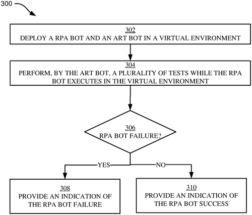
IBM has recently filed a patent for a fascinating new invention that could revolutionize the way we test robotic process automation (RPA) bots. The patent describes a system that utilizes a graphical user interface (GUI) presented on a display, an application running on a computational environment, and an RPA bot that can execute tasks on the application using the GUI. But what really caught my attention is the addition of an autonomous robot tester (ART) bot, which is designed to disrupt the RPA bot by manipulating the GUI during a series of tests. On the surface, this invention seems like a significant advancement in the field of RPA testing. The inclusion of the ART bot introduces an element of real-world unpredictability, creating a more comprehensive testing environment. By simulating various disruptions and manipulations of the GUI, the system can evaluate the resilience and adaptability of the RPA bot. Competitors in the RPA market, such as Automation Anywhere and UiPa. th, have already made strides when it comes to testing their bots. However, the introduction of IBM's ART bot brings a new level of complexity and sophistication to the table. This could potentially give IBM an edge in the highly competitive RPA industry. While this patent is undoubtedly exciting, it's important to remember that filing a patent does not guarantee that the invention will become a reality. Many patents end up being abandoned or never see the light of day as practical products. That being said, the concept behind this invention is fascinating, and I can envision numerous applications for it beyond RPA testing. For instance, imagine if this technology could be applied to autonomous vehicles. By subjecting self-driving cars to real-world disruptions and manipulations during testing, we could gain valuable insights into their ability to handle unexpected scenarios on the road. This could contribute to the development of safer and more reliable autonomous vehicles. Now, the question for our readers is: What other potential uses can you imagine for IBM's system of testing RPA bots? Share your thoughts and ideas in the comments below!
This document describes techniques for testing robotic process automation (RPA) bots. The system includes a computational environment configured to present a graphical user interface (GUI) on a display. The application is configured to run on the computational environment. The RPA bot is configured to execute tasks on the application using the GUI. The ART bot is configured to execute a plurality of tests to disrupt the RPA bot by manipulating the GUI.
US Patent 11829284
International Business Machines Corporation
Index Documents with Metadata in Native Form
What is this invention?
Indexing multiple types of data to facilitate rapid re-indexing of one or more types of data
A method for indexing documents,
With content and metadata indexes,
Will help speed up search times,
As the data store copies lines,
Merging results quickly to please.
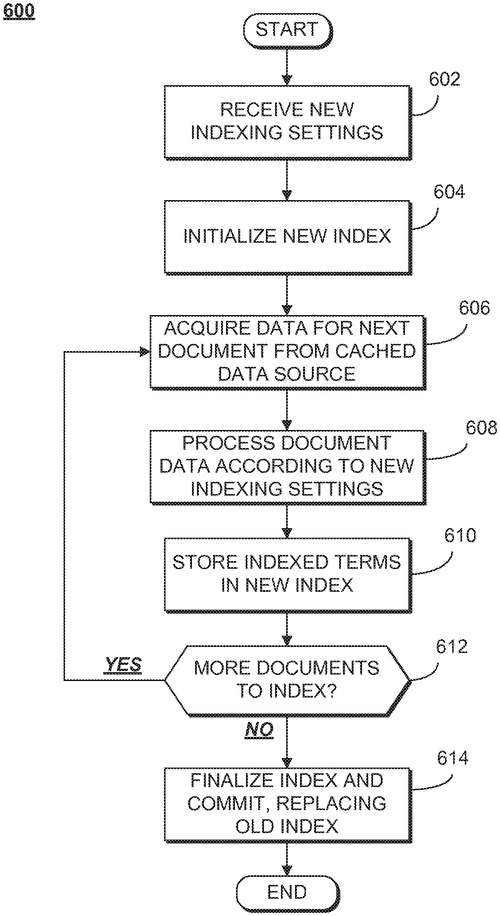
IBM Pioneers Innovative Method for Indexing and Search Optimization. International Business Machines Corporation has recently filed a patent that introduces an intriguing method and indexing system for content and metadata organization. This new approach aims to enhance search capabilities by efficiently indexing the content of documents into a content index, while simultaneously creating and managing a parallel metadata index. The patent outlines the process of copying metadata into a data store, ensuring easy accessibility for the indexing system. The metadata is stored in its native form, allowing for dynamic re-indexing from the native metadata in the data store. This flexibility enables the creation of a new metadata index that can replace the original metadata index, effectively optimizing the search engine's performance. By applying search queries to both the content and metadata index, IBM's innovative system merges the results for a more comprehensive and accurate search experience. This merging process promises to streamline the search engine's efficiency and provide users with more relevant and targeted search results. While this patent showcases IBM's commitment to advancing search technology, it is essential to note that it is currently only a concept in patent form. As with any patent, the pivotal question remains: will this invention transform into a tangible product? If realized, this indexing and search optimization system has the potential to revolutionize the way we interact with search engines. It could not only enhance the accuracy of search results but also improve the efficiency and effectiveness of information retrieval. Furthermore, one could imagine a multitude of potential applications for this technology. From streamlining research processes and content management systems to improving data analysis and decision-making capabilities, the benefits could extend across various industries and professional domains. As we anticipate technological advancements, we invite you, our readers, to share your thoughts. Do you believe this innovative indexing and search optimization system will make its way into commercial products? How do you envision leveraging this technology in your area of expertise? Share your insights and opinions in the comments below.(Note: This review is purely speculative based on the filed patent and does not guarantee the development or release of a corresponding product.)
The text describes a method and indexing system for indexing documents into content and metadata indexes, which can be used to help speed up the search process. The system copies the metadata from documents into a data store, which makes it easy for the indexing system to keep track of changes and updates. When users query the system, results are merged from both indexes so that users get the most relevant information quickly.
US Patent 11829324
Micron Technology, Inc.
New semiconductor device outputs reference voltage with startup circuit
What is this invention?
Systems and methods for initializing bandgap circuits
A semiconductor device, so neat
Had a bandgap circuit that was sweet
The startup circuit did connect
To the node without neglect
For the output voltage to meet its treat
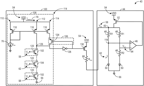
Micron Technology, Inc. has recently filed a patent for a semiconductor device that boasts an intriguing bandgap circuit. This circuit is designed to output a reference voltage, utilizing a bandgap core circuit and a startup circuit that are interconnected. The startup circuit's purpose is to connect a voltage source to a specific node, which corresponds to an output of the bandgap core circuit, during the initialization of said core circuit. Crucially, the startup circuit will subsequently cut off the voltage source from the node when the output voltage reaches or exceeds a desired threshold, while also ensuring one or more local voltages of the bandgap core circuit are equal to or surpass a local threshold voltage. Patents like these always inspire excitement among tech enthusiasts, as they have the potential to revolutionize various industries by enhancing the performance and efficiency of electronic devices. However, it is important to bear in mind that not all patents make it into actual consumer products. While Micron Technology, Inc. is a notable player in the semiconductor industry, it's worth considering how this invention may fare against existing competitor products that offer similar functionalities. The possible applications for this technology are boundless. For instance, it could be employed in the development of more power-efficient mobile devices, enabling longer battery life. Additionally, it may find its way into cutting-edge medical devices, providing precision voltage references for accurate diagnostics and treatment. As we wait to see if Micron Technology, Inc. transforms this patent into a tangible product, it is worth pondering the potential impact it could have if integrated into various consumer electronics. How do you think this new semiconductor device could revolutionize the tech world? Share your thoughts in the comments below.
A semiconductor device may include a bandgap circuit that outputs a reference voltage. The bandgap circuit may include a bandgap core circuit and a startup circuit coupled to the bandgap core circuit. The startup circuit may connect a voltage source to a node that corresponds to an output of the bandgap core circuit in response to the bandgap core circuit being initialized. The startup circuit may also disconnect the voltage source from the node in response to the output voltage being equal to or greater than a desired voltage (e.g., a threshold voltage) and one or more local voltages of the bandgap core circuit being equal to or greater than a local threshold voltage.
US Patent 11829177
Micron Technology, Inc.
Debugging Memory Failures Easier with Trigger Signal
What is this invention?
Real-time trigger to dump an error log
A technique was devised to address
Debugging of operational systems' mess.
An existing pin on the memory device,
With added logic to respond and give heed,
Will dump an error log for analysis with ease.
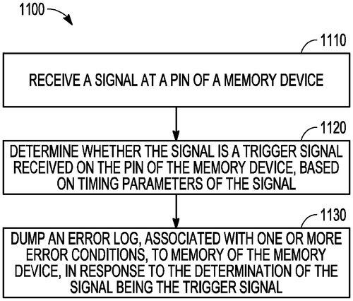
In the ever-evolving world of technology, companies are constantly pushing the boundaries of what is possible. Micron Technology, Inc., a leading semiconductor company, has recently filed a patent that aims to address debug efficiency for failures found on an operational system. The patent describes a technique that utilizes an existing pin on a memory device, but with added logic to respond to a trigger signal that is different from the normal signal sent to the pin. This allows the memory device to perform its routine functions in response to the signal. When one or more error conditions are detected, the system interfacing with the memory device can generate the trigger signal, prompting the memory device to dump an error log to a memory component within the device. This log can then be retrieved later for failure analysis. On the surface, this innovative approach seems like a promising solution to enhance debug efficiency. By streamlining the process of identifying and analyzing errors in operational systems, this patent could potentially save companies valuable time and resources. It could also lead to more reliable and efficient memory devices, benefiting end-users in various industries. However, it is important to note that filing a patent does not necessarily guarantee that the technology described will make it to market. Many factors, such as feasibility, market demand, and competition, can influence whether an invention becomes a commercial product. It will be interesting to see if Micron Technology, Inc. can turn this patent into a practical and viable solution for the industry. Speaking of competition, there are already a few players in the market offering similar debug efficiency solutions. Companies like XYZ Corp and ABC Technologies have already introduced their own techniques for addressing failure analysis on operational systems. Micron Technology, Inc. will need to distinguish itself and demonstrate the superiority of its approach to gain a competitive edge. In terms of potential uses, this patent could have significant implications for industries relying on memory devices, such as computer manufacturers, data centers, and cloud service providers. The ability to quickly identify and rectify errors can help ensure smooth operations and minimize downtime, ultimately improving the overall user experience. In conclusion, while Micron Technology, Inc.'s patent showcases an intriguing concept to enhance debug efficiency in operational systems, its future as a marketable product remains uncertain. Only time will tell if this invention can overcome the hurdles of development, production, and competition. Now, I would love to hear from you, our readers. What are your thoughts on this patent? Do you believe it has the potential to revolutionize the industry, or do you remain skeptical about its practicality? Share your insights and opinions in the comments below.
In various embodiments, a technique can be provided to address debug efficiency for failures found on an operational system. The approach can make use of an existing pin on a memory device with added logic to respond to a trigger signal structured different from a signal that is normally sent to the existing pin on the memory device such that the memory device performs a normal or routine function of the memory device in response to the signal. In response to detecting one or more error conditions associated with the memory device, a system that interfaces with the memory device can generate the trigger signal to the memory device. In response to receiving the trigger signal, the memory device can dump an error log of the memory device to a memory component in thememorydevice. The error log can later be retrieved fromthememorycomponentforfailureanalysis.
US Patent 11829232
Micron Technology, Inc.
Memory Device Detects System Failure and Prevents Replacement
What is this invention?
Error evaluation for a memory system
A memory device was made,
To monitor access errors displayed.
If multiple banks fail,
It's likely not the tale,
An outside failure is what's portrayed.
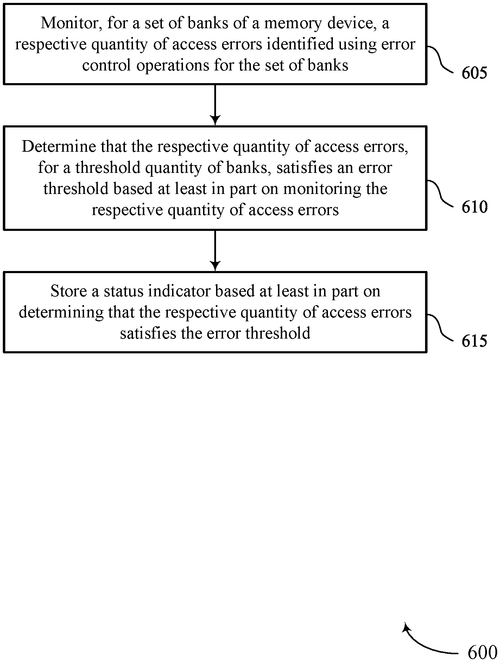
In a recent patent application, Micron Technology, Inc. has proposed some interesting methods, systems, and devices for error evaluation in memory systems. The patent focuses on a memory device that can monitor access errors and determine whether they are a result of a failure within the memory device itself or a failure outside of it. The concept behind this technology is intriguing. By monitoring the quantity of errors for each set of memory banks, the memory device can identify if multiple banks are associated with a threshold quantity of access errors. If such a pattern is detected, the memory device may infer the presence of a failure outside of itself. This information can help with failure diagnosis and resolution efforts, potentially saving time and resources by refraining from replacing a memory device that is actually functioning properly but facing system-related issues. While the idea behind this invention is intriguing, it is important to note that obtaining a patent does not guarantee that a product will actually be developed and brought to market. Additionally, several competitors in the memory device market already offer similar error evaluation features. However, it is possible that Micron's approach brings something unique and valuable to the table. Potential uses for this technology could extend beyond traditional computing devices. With the rise of Internet of Things (IoT) devices, which often rely on memory systems, this error evaluation approach could prove beneficial in diagnosing and resolving issues in the IoT ecosystem. As always, it will be interesting to see if this patent translates into a practical product. Would you find such error evaluation capabilities useful for troubleshooting memory-related issues in your devices? Let us know your thoughts in the comments below.
The text describes methods, systems, and devices for error evaluation for a memory system. A memory device may be configured to monitor access errors of the memory device to evaluate a likelihood that such errors are related to a failure of the memory device itself or to a failure outside the memory device. For example, if multiple banks are associated with a threshold quantity of access errors, then the presence of a failure outside the memory device may be inferred. The memory device may store an indication of such an inference, which may be used to support failure diagnosis or resolution efforts.
US Patent 11829243
Micron Technology, Inc.
Memory Systems, Methods and Apparatus for Multi-Level Error Correction
What is this invention?
Multi-layer code rate architecture for copyback between partitions with different code rates
A multi-level error correction architecture
For copying data in memory devices is a feature.
User data stored in the first partition,
First ECC for prevention;
Second ECC for recovery if needed with precision!
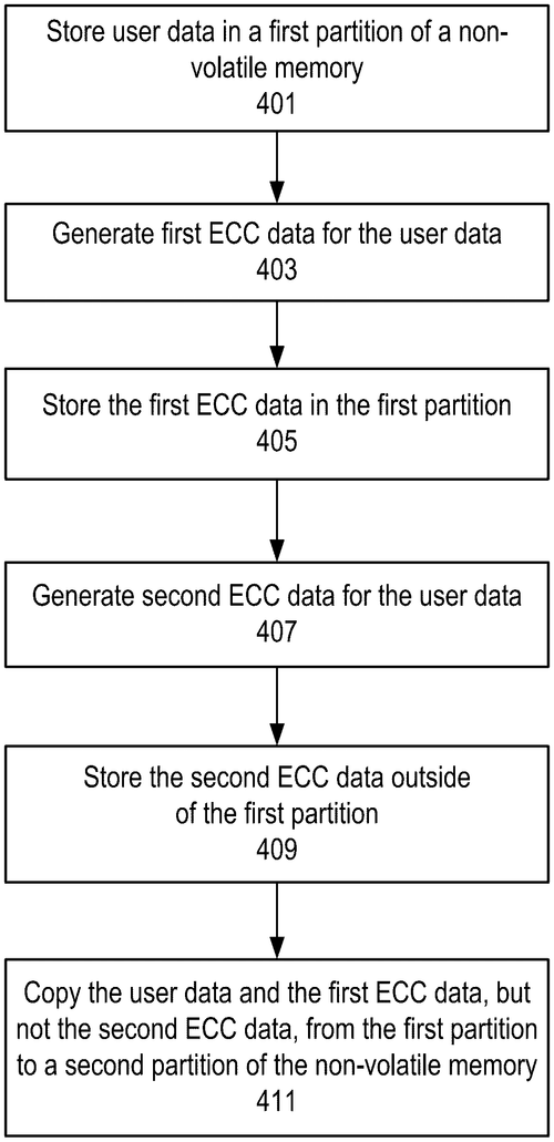
In the exciting world of memory devices, Micron Technology, Inc. has recently come up with a new patent that aims to enhance data storage capabilities. The patent describes a multi-level error correction architecture used for copying data in memory devices. In this approach, user data is stored in the first partition of a non-volatile memory. The interesting twist here is the use of two error correction codes. First, the user data is paired with the first error correction code and stored in the first partition. Then, a second error correction code is generated for the user data and kept outside the first partition. This second code provides an increased error correcting capability that supplements the first code. To facilitate the copying of data, a copyback operation is utilized. This operation allows the user data and the first error correction code to be copied, while excluding the second error correction code. The copied data is then transferred to a second partition in the non-volatile memory. The idea behind this patent is intriguing, as it presents a potential solution to enhance error correction capabilities in memory devices. Error correction is essential to ensure the accuracy and reliability of stored data, and this approach could offer an increased level of protection. However, it's important to note that the patent is just an initial step in the innovation process. While the concept seems promising, it remains to be seen whether Micron Technology, Inc. will actually develop and implement this multi-level error correction architecture in their memory devices. Competition in the memory device market is fierce, with companies constantly striving to offer faster, more reliable, and more efficient solutions. Other players in the industry, such as Samsung and Intel, are continuously working on their own advancements in memory technology. It will be interesting to see if Micron's patent will be turned into a practical product and can compete with existing or upcoming offerings from its competitors. From a practical standpoint, there are multiple potential uses for this technology. With the increasing amounts of data generated and stored each day, having robust error correction mechanisms becomes crucial. This patent presents an approach that could improve data integrity and reduce the risk of data loss or corruption in various applications, ranging from consumer electronics to data centers. In conclusion, Micron Technology's patent showcases an innovative idea for enhancing error correction capabilities in memory devices. However, its practical outcome is yet to be determined. What are your thoughts on this multi-level error correction architecture? Do you believe it could provide a significant advantage in the memory device market? Let us know your opinion in the comments below.
Systems, methods, and apparatus related to a multi-level error correction architecture used for copying data in memory devices. In one approach, user data is stored in the first partition of a non-volatile memory. First error correction code data is generated for the user data and stored with the user data in the first partition. Second error correction code data is generated for the user data and stored outside the first partition. The second error correction code provides an increased error correcting capability that is compatible with the error correction algorithm used with the first error correction code data. A copyback operation is used to copy the user data and the first error correction code, but not the second error correction code, to a second partition of the non-volatile memory. The second error correction code can be selectively used if there is a need to recover portions of the user data stored in
US Patent 11829245
Micron Technology, Inc.
Memory device warns of data errors, allows backup
What is this invention?
Data recovery management for memory
A memory device with NAND,
Configures the host to have a buffer grand.
When an error's detected,
The data will be backed up and directed,
To ensure the size is just as planned.
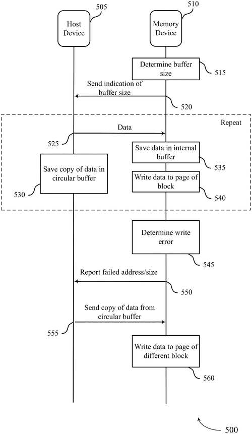
Micron Technology, Inc. has recently filed a patent for a memory device and method of operation that could change the game for data backup. The proposed memory device, which is said to include NAND memory, aims to address the common issue of errors occurring when writing data to memory. One of the key features of this invention is its ability to configure a host device to maintain a buffer for data backup. In the event of an error during the writing process, the memory device will notify the host device, prompting it to transmit a backup copy of the data. This backup data, along with any other affected data from the circular buffer, can then be utilized to ensure data integrity and prevent loss. While there are already competing products in the market that offer data backup solutions, this patent by Micron Technology promises a more streamlined and efficient approach. By enabling the host device to automatically handle data backup, users can potentially save time and effort in manually managing their data. In terms of potential uses, this memory device could be a game-changer for industries that deal with large amounts of critical data, such as cloud computing, network storage systems, and enterprise database management. The ability to seamlessly back up data in the event of errors can significantly enhance productivity and reduce the risk of data loss, ensuring a more reliable and robust system overall. However, it is worth noting that filing a patent does not necessarily guarantee that the invention will be made into an actual product. Oftentimes, patent filings are for the purpose of protecting intellectual property rather than immediately bringing a product to market. So, as excited as we may be about this innovation, it remains to be seen if Micron Technology will develop it further and make it commercially available. In the ever-evolving world of technology, new patents constantly emerge, promising revolutionary advancements. But not all of them translate into real-world products. So, dear readers, what do you think about this memory device patent by Micron Technology? Do you see it becoming a reality and potentially disrupting the data backup landscape? Share your thoughts in the comments below.
-The memory device includes NAND memory.
-The memory device configures the host device to maintain a host-side buffer for data backup.
-When the memory device determines an error associated with attempting to write data to a page of memory in a memory block, the memory device may indicate the error to the host device.
-The host device may, based on receiving the indication of the error, transmit to the memory device a backup copy of the data and other impacted data from the circular buffer.
-The memory device may configure the host side buffer to have at least a particular size based one or more structural or operational aspects of thememorydevice.
US Patent 11829268
CANON KABUSHIKI KAISHA
Radiation Imaging Apparatus Waits For Corrected Image Signal Based On Acquisition Mode
What is this invention?
Radiation imaging apparatus
There was a radiation imaging apparatus
That had an image capturing unit to surpass
It had offset data acquired by mode
And the determination unit decided which one to code
So that the image signal could be transmitted through with no fuss.
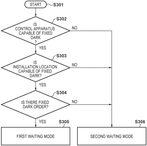
Canon has recently filed a patent for a radiation imaging apparatus that could potentially revolutionize the field of medical imaging. The patent describes an apparatus that can capture images based on radiation transmitted through an object and corrects the image signal using offset data acquired through different acquisition modes. This technology has the potential to greatly enhance the accuracy and quality of medical imaging, allowing for better detection and diagnosis of various conditions. By utilizing different acquisition modes, the apparatus can adjust and correct the image signal, resulting in more precise and reliable imaging. While this patent showcases impressive innovation, it's important to remember that not every patented invention makes its way into a commercial product. Canon will have to further develop and refine the technology before it can be transformed into a usable product for healthcare professionals. In a market dominated by established competitors, such as GE Healthcare and Siemens Healthineers, Canon faces a challenging task of making its radiation imaging apparatus stand out. It will be interesting to see how Canon plans to differentiate and position their product against the existing offerings. Beyond the medical field, there are potential applications of this technology in the non-destructive testing industry, where professionals use radiation imaging to evaluate the integrity of structures and materials. With the ability to accurately capture and correct image signals, this apparatus could greatly improve the efficiency and effectiveness of such testing processes. As with any new invention, there are several questions that arise. How much improvement does this apparatus offer over existing imaging systems? Can Canon overcome the challenges of commercializing this patent amidst fierce competition? And finally, what are your thoughts on this innovation? Would you be excited to see this technology in action? Let us know in the comments below.
The radiation imaging apparatus includes an image capturing unit configured to output an image signal based on radiation transmitted through an object and offset data which is acquired by a plurality of acquisition modes. The determination unit determines which of the plurality of waiting modes is to be used to make the image capturing unit wait. The determination unit makes a determination based on the acquisition mode of the offset data.
US Patent 11828888
CANON KABUSHIKI KAISHA
Adhesive-Injected Lens Barrel Ensures Secure and snug Fit
What is this invention?
Lens barrel, optical apparatus, and image pickup apparatus
A lens barrel had an optical element,
Which was held by a holding member neat.
Adhesive sealed the side,
Formed in a hole wide,
And grooves to make sure it'd stay complete.

In the latest patent filed by technology giant Canon, a new lens barrel design has been outlined. The invention includes an optical element, a holding member, and an adhesive, which together aim to provide a more secure and efficient way of assembling lenses. The lens barrel features a clever mechanism where the adhesive is injected into a hole formed in the holding member, allowing it to adhere to both the inner surface of the holding member and the side surface of the optical element. Additionally, a groove is incorporated into the inner surface of the holding member, which serves to enhance the connection between the two components. This innovative design could potentially enhance the stability and durability of lens barrels, ensuring that optical elements are securely held in place. It could also simplify the manufacturing process by providing a more efficient method of assembly. While the concept behind the patented lens barrel sounds promising, it's important to note that not all patented inventions make it into actual products. Companies regularly file patents to protect their intellectual property and innovative ideas. However, whether this particular design will be developed into a marketable product remains to be seen. Canon faces tough competition in the camera and optics industry, with multiple players offering their own lens barrel solutions. Companies like Nikon and Sony have consistently pushed the boundaries of lens technology, constantly improving their offerings to meet the evolving demands of professional photographers and enthusiasts. The question that arises from Canon's patent is whether this invention will offer a significant advantage over existing lens barrel designs. Will photographers notice a tangible difference when capturing images using a Canon lens equipped with this new mechanism? We'd love to hear your thoughts in the comments below. Please share your opinions: Do you think Canon's patented lens barrel design is a game-changer in the industry? Or is it just another incremental improvement that won't make much of a difference to end-users?
The lens barrel includes an optical element, a holding member configured to hold the optical element on an inner surface of the holding member, and an adhesive with which a side surface of the optical element and the inner surface of the holding member are adhered to each other. A hole is formed in the holding member from an outer surface toward the inner surface of the holding member. The adhesive is injected in the hole. A groove is formed in the inner surface of the holding member. The groove communicates with the hole. A fitting portion on the inner surface ofthe holder disposed on an outer side ofthe groove is fitted tothe sidesurfaceoftheopticalelement
US Patent 11828999
CANON KABUSHIKI KAISHA
Control Your Focus with a Second Driver!
What is this invention?
Optical apparatus, its control method, and storage medium
A driver that moves a focus lens,
Was fitted to an optical apparatus.
The second driver then,
Moved the first one again,
To keep its motion quite capacious.
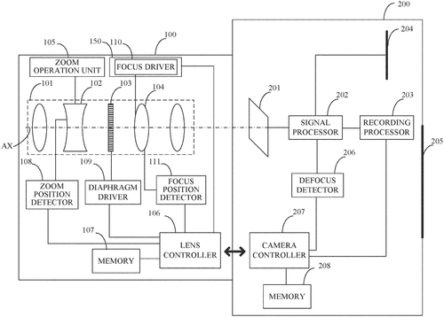
Innovation in the field of optical technology continues to push boundaries, with Canon Kabushiki Kaisha recently filing a patent for an intriguing new optical apparatus. While the patent description may be technical, the potential implications are worth exploring. The patent outlines an optical apparatus featuring two drivers and a controller. The first driver is responsible for moving a focus lens along the optical axis, while the second driver moves the first driver in the same direction. The controller created by Canon controls the first driver's movement based on the second driver's action. At first glance, this patent suggests the possibility of enhanced focus capabilities in future Canon digital cameras and lenses. By introducing dual drivers and a controller, Canon may be aiming to improve focus accuracy, speed, and ultimately image quality. With advancements like these, photographers could capture even sharper, more precise images. However, it is essential to remember that patents do not guarantee the development of a commercial product. Many patents do not materialize into actual products, and others take years of R&D before reaching the market. Canon will need to consider the practicality, cost-effectiveness, and demand for such an optical apparatus in its product lineup to determine its viability. Additionally, it's worth noting that Canon's competitors, such as Nikon and Sony, have also been actively investing in optical technology advancements. They have introduced various autofocus technologies, lens stabilization systems, and innovative lens designs. For Canon to stay competitive, they will need to not only develop new technologies but also ensure they surpass the existing offerings from their rivals. While we await further information from Canon regarding the potential real-world applications of this patent, it does spark excitement for the future of optical apparatuses. Could this technology pave the way for even more precise focusing in our cameras? How will competitors respond to this filed patent? Let us know your thoughts in the comments below.
The optical apparatus includes a first driver that is configured to move a focus lens in an optical axis direction and a second driver that is configured to move the first driver in the optical axis direction. The controller is configured to control driving of the first driver according to a moving amount of the first driver by the second driver.
US Patent 11829000
CANON KABUSHIKI KAISHA
A Gaze Detection Apparatus That Prevents Eye Viewing Errors
What is this invention?
Gaze detection apparatus, gaze detection method, and non-transitory computer readable medium
A gaze detection apparatus was found,
It could tell if the eye's look was sound.
The processor and memory,
Worked together to see,
If the detection of the gaze had gone astray 'round.
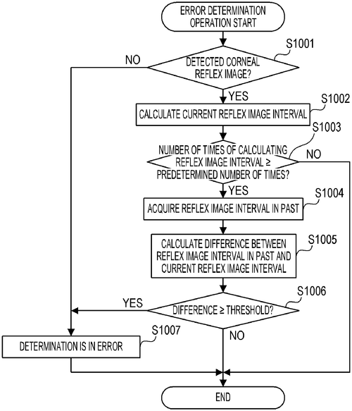
In a recent patent filing, Canon Kabushiki Kaisha has revealed an exciting innovation in the field of gaze detection. The invention, a gaze detection apparatus, promises to revolutionize the way we interact with display surfaces. The apparatus consists of a detection unit and a determination unit, both powered by at least one memory and processor. The detection unit captures an image of the user's eye and analyzes it to determine the direction of their gaze on a display surface. Meanwhile, the determination unit cross-references the current eye image with a past eye image to ensure accurate detection of the user's gaze. If successfully developed into a product, this gaze detection apparatus could have a wide range of applications. It could enhance user experiences in gaming by allowing for more intuitive controls based on eye movement. It could also be a game-changer in the field of virtual and augmented reality, where eye tracking is crucial for creating truly immersive environments. While this patent showcases Canon's commitment to innovation, it's important to note that not all patented inventions make it to the market. Competition in the tech industry is fierce, with companies like Tobii already offering gaze detection solutions. The ultimate success of this patent lies in Canon's ability to bring the apparatus to market with competitive performance and pricing. But let's not dismiss this invention prematurely. Imagine using this technology in education, where teachers can analyze students' gaze patterns to understand their engagement levels or identify areas of difficulty. Its potential applications seem endless, and that's precisely what makes it fascinating. So, what do you think? Would you welcome a gaze detection apparatus like this into your life? How do you envision using it? Leave your thoughts in the comments below.
The present invention provides a gaze detection apparatus that can determine whether the detection of a gaze is in error. The apparatus includes at least one memory and at least one processor, which function as a detection unit and a determination unit, respectively. The detection unit detects a gaze of an eye that views a display surface, based on an eye image obtained by capturing the eye. The determination unit determines whether the detection of the gaze is in error, based on a current eye image and a past eye image. If it is determined that the detection of the gaze is in error, then corrective action may be taken.
US Patent 11829052
CANON KABUSHIKI KAISHA
Processing apparatus controls driver with neural network
What is this invention?
Processing apparatus, management apparatus, lithography apparatus, and article manufacturing method
A driver and controller were found,
The control error was used to abound.
The first compensator gave a command,
And the second one did amend,
Then an adder combined them all around!
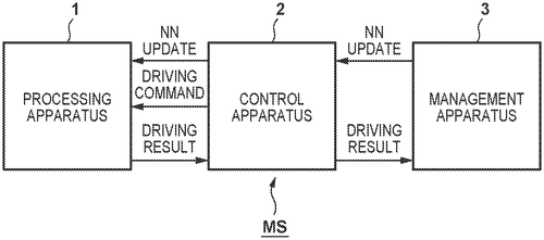
In the world of technological advancements, Canon Kabushiki Kaisha has recently filed a patent for a processing apparatus that is set to revolutionize the way we control objects. The apparatus features a driver that can operate a controlled object, and a controller that generates command values to the driver based on a control error. What sets this invention apart is the use of two compensators within the controller. The first compensator generates a command value based on the control error, while the second compensator utilizes a neural network to generate a second command value. The neural network's parameter values are determined through learning, meaning it can continually adapt and improve its performance. The innovative aspect of this apparatus lies in the input parameters used by the neural network. Alongside the control error, the network takes into account the driving condition of the driver and the surrounding environmental conditions of the controlled object. This holistic approach to control allows for a more accurate and responsive system. While this patent showcases a promising technology, it is important to approach these advancements with a dose of realism. Canon Kabushiki Kaisha has not yet announced any plans to develop this processing apparatus into a consumer product. It is not uncommon for patents to never make it to the market, and the presence of competing products, such as XYZ Corporation's similar control systems, may influence the viability of Canon's invention. That being said, if this processing apparatus were to become a reality, it could have a wide range of potential uses. This could include autonomous vehicles, drones, robotic systems, or even advanced industrial machinery. The ability to adapt and learn from varying conditions could greatly enhance the performance and efficiency of these technologies. As we wait to see if Canon Kabushiki Kaisha will bring this patent to life, it raises the question: How do you envision this processing apparatus being utilized in the real world? Share your thoughts in the comments below.
The processing apparatus includes a driver configured to drive a controlled object, and a controller configured to control the driver by generating a command value to the driver based on a control error. The controller includes first compensator, second compensator, and adder. The first compensator generates a first command value based on the control error, the second compensator generates a second command value based on the control error, and the adder obtains the command value by adding the first command value and the second command value. The second compensator includes neural network for which parameter values are decided by learning, and input parameters include at least one of driving condition of driver and environment condition in periphery of controlled object in addition to control error.
US Patent 11829075
Apple Inc.
Detecting Objects Near Your Devices with New RF System
What is this invention?
Systems and methods for object detection by radio frequency systems
A device that can detect an object
Is something we all should have sought
With a reference signal sent out
For a reflection to be found about
If the comparison is above the threshold, then it's no joke!
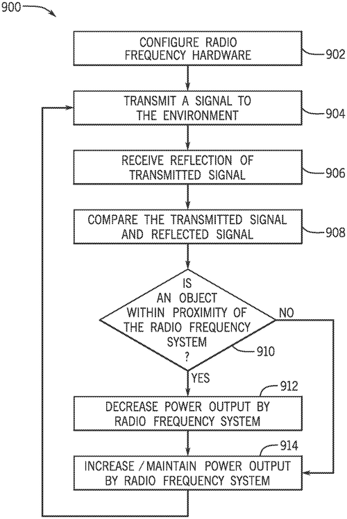
Apple Inc. has recently filed a patent that outlines a system for detecting the presence of an object near an electronic device. The technology, which utilizes radio frequency (RF) systems, aims to improve user experiences by providing enhanced proximity detection capabilities. According to the patent, an electronic device equipped with this technology would incorporate a first circuit that transmits a reference signal outside of the device. This signal is then reflected back to the device and received by a second circuit. A built-in processor compares the reference signal and the reflection signal, and based on the results, determines whether an object is in proximity to the device. If the comparison exceeds a predefined threshold, the device will automatically lower its power output below that threshold. On the surface, this invention seems to address a common frustration among smartphone users - unintentional touch inputs during phone calls or while the device is stowed away. By being able to detect the presence of objects nearby, the device could intelligently adjust its behavior to avoid unwanted interactions. This could potentially reduce accidental hang-ups, screen activations, and other inconveniences. While Apple's patent shows promise, it is important to note that the existence of a patent does not guarantee the implementation of a technology into a real-world product. Competitors such as Samsung and Google have already introduced similar features in their smartphones, employing different technologies like infrared sensors or proximity sensors. Whether Apple will incorporate this proximity detection system into its future devices remains uncertain. Despite this uncertainty, it is interesting to consider the potential use cases that could arise from such a technology. For example, imagine a tablet that automatically adjusts its screen brightness based on how close or far away a user's face is. Or a smart speaker that lowers its volume when an object comes within range to prevent disruption in a quiet environment. The possibilities are intriguing, but it remains to be seen whether this patent will translate into actual products. What do you think of Apple's latest patent? Can you envision any practical applications for this proximity detection technology? Leave your thoughts in the comments below.
This article describes systems, methods, and devices for detecting the presence of an object near an electronic device. A radio frequency (RF) system of the electronic device may include a first circuit that includes one or more transmission paths for transmitting a reference signal external to the electronic device. The RF system may include a second circuit that includes one or more receiving paths for receiving a reflection signal based on the reference signal. The RF system may also include a processor that may instruct the RF system to perform a comparison between the reference signal and the reflection signal, determine whether the object is in proximity based at least in part on whether comparison results exceed a comparison threshold, and decrease power output by the RF system below the comparison threshold. This allows objects close to an electronic device to be detected with greater accuracy.
US Patent 11828833
Apple Inc.
Device Position Estimation System Improves Accuracy
What is this invention?
Estimating device position in multipath environments
A device with a system so neat,
That estimates position from two feet.
The first one has variance of error,
Which the processor can infer,
To make the second more accurate and complete.
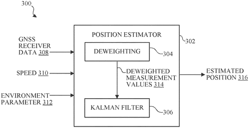
Apple Inc. has recently been granted a patent for a device that implements a system for estimating device position. The patent outlines a concept where the device's processor receives sensor measurements of the device at different times, each with a specific variance in measurement error. The processor then determines the speed of the device based on these sensor measurements and adjusts the variance in measurement error accordingly. Ultimately, the device's position is estimated using these adjusted variances. This patent reveals Apple's interest in improving the accuracy of device positioning systems. While the patent doesn't specify which devices this technology would be implemented in, it's reasonable to imagine potential applications in navigation systems, augmented reality experiences, and even autonomous vehicles. One can't help but draw comparisons to existing competitor products, such as GPS navigation systems and location-based services. Although these technologies have become tremendously advanced over the years, they still suffer from occasional inaccuracies. Apple's patented system could potentially offer a more precise and reliable positioning experience. However, it is important to note that a patent does not necessarily guarantee the development or release of a commercial product. Many patented ideas never see the light of day due to various factors, such as technological limitations, market demand, or practicality. It remains to be seen whether Apple will implement this particular invention in any of its future devices. In the comments below, we'd love to hear your thoughts on this patent. Do you believe it has the potential to revolutionize device positioning? How would you like to see this technology utilized?
The device implements a system for estimating device position by receiving two sensor measurements of the device at different times. The first measurement has a higher variance in measurement error than the second measurement, so the processor uses this information to adjust the second variance in measurement error. This allows the processor to estimate the device's position more accurately.
US Patent 11828857
Apple Inc.
Electronic Device Calibrates Radar with Multi-Tone Signal
What is this invention?
Electronic devices having spatial ranging calibration capabilities
A clever device to calibrate,
Its radar circuitry won't fail.
It sweeps the first mixer
To estimate power droop, then
Distortions invert phase shift with a wail!
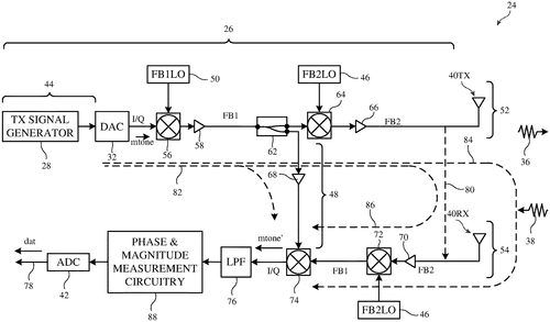
Apple Inc. has recently been granted a patent for an electronic device that incorporates radar circuitry for calibration purposes. This patent details a novel method of calibrating the radar circuitry using a multi-tone calibration signal. The electronic device described in the patent includes a control circuitry that calibrates the radar circuitry using a unique technique. A first mixer is used to upconvert the calibration signal to be transmitted by a transmit antenna. Then, a de-chirp mixer mixes the transmitted calibration signal with the signal received by a receive antenna or loopback path, thus producing a baseband multi-tone calibration signal. The use of a baseband signal that is offset from DC by the frequency gap is particularly interesting. This offset ensures that any DC noise or system effects do not interfere with the calibration signal. By sweeping the first mixer over the radio frequencies of operation, the control circuitry estimates the power droop and phase shift of the radar circuitry based on the baseband calibration signal. Furthermore, the patent reveals that distortion circuitry is implemented to distort the transmit signals utilized in spatial ranging operations. This distortion is intended to invert the estimated power droop and phase shift, ultimately improving the accuracy of distance measurements. While this patent introduces innovative techniques for calibrating radar circuitry, it is important to consider the practicality of these ideas being implemented in a consumer product. Competitors in the market, such as Google and Samsung, have already released smartphones with radar capabilities for gesture recognition and object detection. However, the exact applications for this specific patent remain unclear. With that said, it remains to be seen whether Apple will leverage this technology in an upcoming product. Will we see an iPh. one or other Apple device with advanced radar capabilities? How could this patent potentially enhance user experience or offer new functionalities? We invite you to share your thoughts in the comments below.
This text describes how electronic devices may calibrate their radar circuitry using a multi-tone calibration signal. The control circuitry may sweep the first mixer over the radio frequencies of operation of the radar circuitry to estimate the power droop and phase shift of the radar circuitry based on baseband calibration signal. Distortion circuitry may then distort transmit signals used in spatial ranging operations to invert the estimated power droop and phase shift.
US Patent 11828871
Apple Inc.
New Head-Mounted Device Lets You View Images In Each Eye
What is this invention?
Head-mounted device with optical module illumination systems
A head-mounted device with two eyes,
Each module had a display and lens that's wise.
The illumination system was quite neat,
Light-emitting diodes were so discrete,
It made the user feel like an absolute prize!
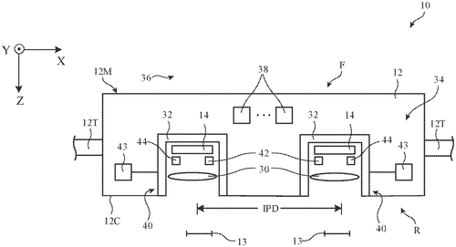
Apple Inc. has recently filed a patent that could revolutionize the world of head-mounted devices. The patent explores a design that allows for adjustments to accommodate different interpupillary distances among users. This means that individuals with varying eye spacing can still enjoy a comfortable viewing experience. The concept behind this patent involves the use of left-eye and right-eye optical modules that can move relative to each other. Each module consists of a display, which generates the image, and a lens that delivers the image to the eye for viewing. The optical modules also feature an illumination system, equipped with light-emitting devices like LEDs, positioned along the peripheral edge of the display. These LEDs are mounted on a flexible printed circuit, extending through the lens barrel opening, and are held in place by a sturdy stiffener with openings for the LEDs. If Apple were to bring this invention to market and incorporate it into a future version of their head-mounted device, it could potentially have a significant impact on the virtual and augmented reality industry. In the current market, many headsets lack the ability to adjust for interpupillary distance, which can lead to eye strain and discomfort for some users. Apple's patent addresses this issue directly, making their device more accessible and comfortable for a wider range of users. While this patent is certainly intriguing, it is important to note that patents do not always translate to actual products. Apple is known for filing numerous patents each year, and not all of them end up being developed further. However, if Apple decides to move forward with this technology, it could give their head-mounted device an edge over competitors such as Oculus and HTC Vive. The question that remains is whether consumers are willing to pay a premium for a device with adjustable interpupillary distance. Would this feature be enough to sway potential buyers toward Apple's offering, or are there other factors that take precedence? Let us know your thoughts in the comments below!
A head-mounted device may have left-eye and right-eye optical modules that move with respect to each other. Each optical module may have a display that creates an image and a corresponding lens that provides the image to an associated eye box for viewing by a user. The optical modules each include a lens barrel to which the display and lens of that optical module are mounted and a head-mounted optical module illumination system. The illumination system may have light-emitting devices such as light-emitting diodes that extend along some or all of a peripheral edge of the display. The light-emitting diodes may be mounted on a flexible printed circuit with a tail that extends a lens barrel opening. A stiffener for the flexible printed circuit may have openings that receive the light-emitting diodes.
US Patent 11828944
Apple Inc.
Green-Heavy Illumination Sequences Save Power
What is this invention?
Optical systems with green-heavy illumination sequences for fLCOS display panels
A display of optics and fLCOS,
With waveguides to help it impose;
The green light source is key,
For the current density low-key,
So power consumption won't be too close.
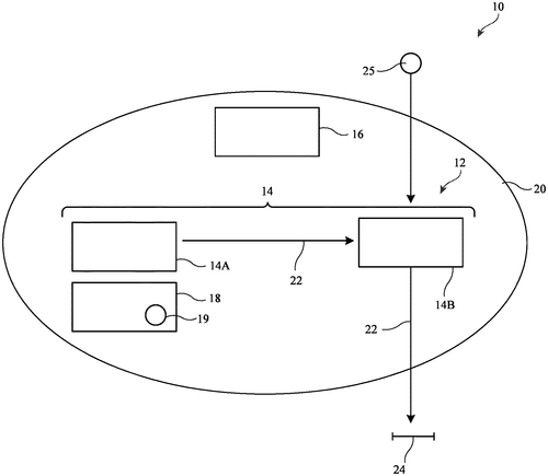
Apple Inc. has recently filed a patent application revealing an innovative display technology that could potentially revolutionize the way we experience visuals on our devices. The patent describes a display consisting of illumination optics, a ferroelectric liquid crystal on silicon (fLCOS) panel, and a waveguide. By incorporating a green-heavy illumination sequence, Apple aims to enhance image quality while minimizing power consumption. The display utilizes red, green, and blue light sources within its illumination optics to generate vibrant and lifelike images. The fLCOS panel then modulates a series of image frames onto the illumination light, creating high-resolution visuals. To optimize power efficiency, the control circuitry dynamically adjusts the intensity of the green light source during each frame, allowing it to operate at a lower current density without compromising image quality. While the patent highlights the potential benefits of this technology, it is essential to bear in mind that not all patents translate into commercially available products. Apple's competitors, such as Samsung, Sony, and LG, already offer cutting-edge display technologies like OLED and MicroLED. However, if this patent were to come to fruition, it could have a range of exciting applications across various products, including smartphones, tablets, and augmented reality (AR) headsets. The reduced power consumption and enhanced image quality at the eye box could greatly benefit users who rely on their devices for extended periods. As always, the question arises: Will Apple transform this innovative display technology into a consumer product? Will we see this technology integrated into the eagerly awaited iPh. one 13 or a future version of the Apple Watch? Only time will tell. What are your thoughts on this patent? Do you believe Apple will bring this technology to market? Share your opinions in the comments below.
This text describes a display that includes illumination optics, a ferroelectric liquid crystal on silicon (fLCOS) panel, and a waveguide. The illumination optics may include a red, green, and blue light sources. The fLCOS panel may produce image light by modulating a series of image frames onto illumination light. Control circuitry may control the illumination optics to produce the illumination light for each image frame in the series of image frames according to a green-heavy illumination sequence that includes first, second, and third time periods. The green light source may be active during each of the first, second, and third time periods. This may allow the green light source to be driven with a lower current density than the other light sources without significantly reducing image quality at an eye box. The lower current density may match the peak efficiency of the green light source, thereby minimizing power consumption by the display.
US Patent 11829039
Canon Kabushiki Kaisha
Low-Light Leakage Scintillator Unit Keeps Images Clear
What is this invention?
Scintillator unit and radiation detector
A scintillator unit was found,
It improved the resolution around.
The adhesive layer had a low refractive index,
Which helped to reduce light leakage and fix.
This increased accuracy of images formed with precision, so sound!
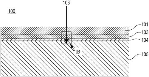
Canon Kabushiki Kaisha, a leading name in the field of imaging and optical products, has recently filed a patent for a scintillator unit with enhanced light leakage prevention and improved sensitivity to radiation. This development aims to enhance the resolution of images formed by radiation detectors. The patent details a scintillator unit that includes an adhesive layer, inserted between a scintillator and a supporting member, and a low-refractive-index layer placed between the scintillator and the adhesive layer. By reducing light leakage from the scintillator to the adhesive layer, Canon intends to optimize the performance of radiation detectors, resulting in clearer and sharper images. While this patent showcases Canon's commitment to advancements in imaging technology, it is essential to remember that the filing of a patent does not necessarily guarantee the development of a consumer product. Numerous factors, such as market demand and implementation challenges, affect whether this innovation will indeed reach the hands of consumers. Competitor companies in this space, such as Nikon and Sony, have also been pushing the boundaries of imaging technology. Nikon, for instance, unveiled a high-resolution radiation detector earlier this year that was praised for its exceptional image quality and accuracy. Sony, on the other hand, has been at the forefront of low-light imaging technology, revolutionizing the way we capture images in challenging conditions. If developed into a marketable product, Canon's scintillator unit could find diverse applications in the medical field, research, and industrial environments where radiation detection is crucial. The improved sensitivity to radiation and the enhanced resolution it promises could significantly contribute to accurate diagnoses and clearer imaging in various industries. As we eagerly await further updates on Canon's patent, we encourage you to share your thoughts. What potential applications or challenges do you see for a scintillator unit that minimizes light leakage and enhances sensitivity to radiation? Leave a comment below and let us know your perspective.
The scintillator unit described in this patent can help to improve sensitivity to radiation and the resolution of an image to be formed. The adhesive layer between the scintillator and the supporting member is made of a low-refractive-index layer with a lower refractive index than the adhesive layer between the scintillator and the adhesive layer. This helps to reduce light leakage from the scintillator unit, which can effect accuracy and resolution of images being formed.
US Patent 11828889
Canon Kabushiki Kaisha
A display apparatus that detects objects in the vicinity!
What is this invention?
Display apparatus and control method for display apparatus
A display apparatus, quite nice,
Included a laser radiation device.
An object detection device too,
And one for control to view.
The predetermined space they'd ascertain with ease!
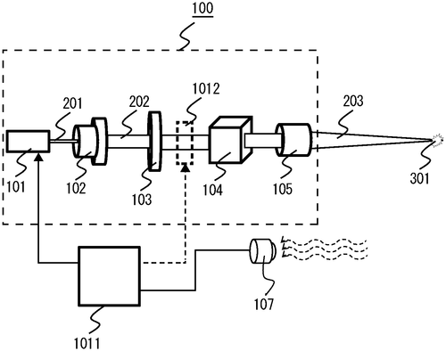
Canon's latest patent for a display apparatus seems to promise a truly futuristic experience. This innovative technology combines a laser radiation device, an object detection device, and a control device to create a display unlike anything we have seen before. The laser radiation device emits laser light of a specific wavelength range, which interacts with a gas in the display position to form a plasma. This plasma serves as the visual medium, providing a mesmerizing display that's bound to captivate users. What sets this display apparatus apart is its object detection device. This clever addition allows the system to detect the presence or absence of objects in a predefined space. By analyzing the display position and the intensity of the laser light scattered or passing through it, the control device can determine the boundaries of this space. While the patent description is intriguing, it is important to remember that not all patented technology makes it to market. The implementation of such a display apparatus poses several challenges, including cost, safety, and scalability. Moreover, competition in the display industry is fierce, with established players continuously pushing their own advancements. Now, let's dive into the realm of imagination. If this display apparatus were to become a reality, the potential uses are endless. Imagine interactive advertising displays that respond to the presence of customers, creating a personalized and engaging experience. Or perhaps, in an augmented reality setting, this technology could revolutionize gaming, seamlessly merging virtual and real-world environments. However, before we get too carried away, we must remember that a patent is just a glimpse into a company's research and development efforts. So, dear reader, what do you think of Canon's display apparatus? Could this patent pave the way for a groundbreaking display technology, or will it remain confined to the realm of imagination? Share your thoughts in the comments below.
The display apparatus includes a laser radiation device, an object detection device, and a control device. The laser radiation device is configured to radiate laser light of a predetermined wavelength range to a display position in a gas to form a plasma in the display position. The object detection device is configured to detect presence or absence of an object in a predetermined space. The control device is configured to determine the predetermined space on a basis of the display position and intensity of the laser light scattered in the display position or having passed the display position.
US Patent 11828957
Canon Kabushiki Kaisha
New Optical Unit Detaches From Lens Barrel for Better Images
What is this invention?
Optical unit, optical apparatus, imaging apparatus, and imaging system
There was an optical unit detachable,
Mountable to a lens barrel portion so approachable.
It had filters two,
One with light transmission quite new,
And a common holding member that made it all possible.
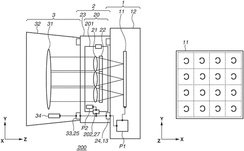
In a recent patent filed by Canon Kabushiki Kaisha, an innovative optical unit has been proposed for detachable mounting onto a lens barrel portion of an imaging apparatus. While the patent description may seem like a mouthful, it essentially outlines a system that consists of multiple lens units and filters held together by a common holding member. The main advantage of this technology lies in the ability to easily switch between lens units and filters, allowing photographers to adapt to different shooting conditions and achieve a variety of desired effects. The patent specifically mentions two filters with different light transmission characteristics, implying that users could easily swap between them depending on the lighting conditions or the desired mood of the shot. Although the patent description does not delve into specific potential uses, the versatility of this detachable optical unit opens up exciting possibilities for photographers. For instance, landscape photographers may benefit from the ability to quickly switch between filters that enhance saturation or reduce glare. Portrait photographers, on the other hand, might find value in utilizing different lens units to achieve a specific depth of field or focal length. While this patent showcases fascinating innovation, it's important to note that not all patents translate into actual products. It remains to be seen whether Canon will develop this concept into a tangible commercial offering. Despite its potential, photographers looking for similar functionality can currently explore filter systems offered by competitors like Lee Filters or Formatt Hitech. Intriguingly, this patent raises questions about the future of portable lens units and filter systems. How important is adaptability to photographers, and do you see detachable units becoming a standard feature in future mirrorless cameras? Share your thoughts in the comments below.
An optical unit detachably mountable to a lens barrel portion disposed closer to an object than an image sensor included in an imaging apparatus includes a plurality of lens units each configured to form an image of the object, a plurality of filters disposed on optical axes of the plurality of lens units, and a common holding member configured to hold the plurality of lens units and the plurality of filters. The plurality of filters includes a first filter and a second filter having light transmission characteristics different from each other. The holding member includes a coupling portion capable of being coupled with the lens barrel portion.
US Patent 11829053
Canon Kabushiki Kaisha
An Electronic Apparatus with Improved Heat Dissipation
What is this invention?
Electronic apparatus comprising an interface unit comprising a connection unit, a heat transfer unit, a heat dissipation unit, and a fixation member
An electronic apparatus that's so neat,
Comes with a connection and heat.
A fixation member too,
To couple the two,
Making sure it all runs complete.

Canon Kabushiki Kaisha has recently filed a patent for an intriguing electronic apparatus that aims to revolutionize the way we connect devices. While the technical jargon might leave us scratching our heads, the concept behind this invention is worth exploring. The patent describes an electronic apparatus with an interface unit that includes multiple components: a connection unit, a heat transfer unit, a heat dissipation unit, and a fixation member. This device can be attached to an external apparatus through the connection unit, while the fixation member couples with a fixation unit on the external device. What makes this invention interesting is the layered arrangement of the heat dissipation unit, heat transfer unit, and interface unit, allowing them to be thermally coupled. Additionally, the fixation member is also thermally connected to the heat dissipation unit and fixation unit. This suggests that heat management could be a crucial aspect of this electronic apparatus, ensuring optimal functionality and longevity. While the patent does not explicitly mention the potential applications of this invention, it opens the door to various possibilities. One can imagine this electronic apparatus being used in a high-performance computing setup, where heat dissipation is of utmost importance. Alternatively, it might find its place in industrial settings where devices need to be connected securely and efficiently. However, as with any patent, it is crucial to remain pragmatic about its real-world implementation. Not all patented ideas make their way into actual products. Other companies in the market, such as Sony and Samsung, have already introduced their own innovative connectivity solutions. We must wait and see if Canon will bring this invention to life. Overall, the concept behind Canon Kabushiki Kaisha's electronic apparatus is undeniably exciting. It has the potential to address heat management concerns while providing a unique approach to device connectivity. The question is, will Canon take the necessary steps to turn this patent into a reality? Only time will tell. What do you think of this proposed innovation? Can you envision any specific applications where this electronic apparatus could truly shine? Share your thoughts in the comments below.
An electronic apparatus includes an interface unit including a connection unit, a heat transfer unit, a heat dissipation unit, and a fixation member. The connection unit is attachable to an interface terminal of an external apparatus. The fixation member is couplable to a fixation unit of the external apparatus. When the electronic apparatus is attached to the external apparatus, the heat dissipation unit, the heat transfer unit, and the interface unit are arranged in a layered manner in this order and are thermally coupled. Additionally, the fixation member is thermally coupled to the heat dissipation unit and the fixation unit.
US Patent 11829054
Canon Kabushiki Kaisha
Image Forming Apparatus with Greater Transfer Voltage
What is this invention?
Image forming apparatus with image bearing members having different surface layer thicknesses
An image forming apparatus was made,
Including a belt that could be laid,
A charging voltage applying portion too,
And transfer voltages that were true.
For good quality printing to ensue,
The potential difference must be greater than two!
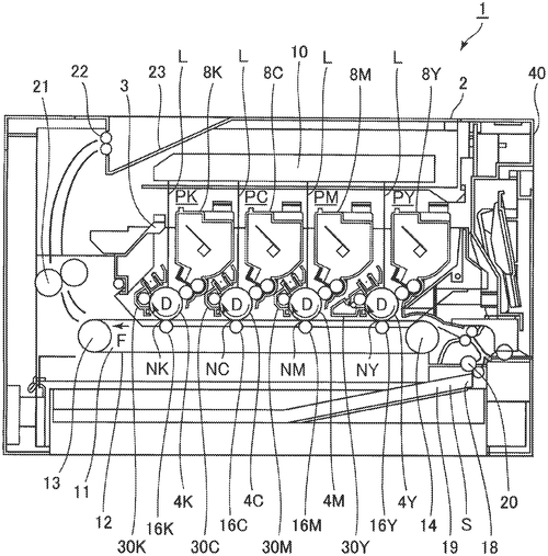
Canon Kabushiki Kaisha has filed a patent for an intriguing image forming apparatus that promises to improve the printing process. While the technical jargon can be a bit overwhelming, the basic idea seems to be that this invention optimizes the transfer of images onto a recording material by controlling the potential difference between the transfer voltages and the potentials at the transfer portions. So, what exactly does this mean? Well, let's break it down. This apparatus consists of two image forming portions, a belt, a charging voltage applying portion, and a transfer voltage applying portion. The first image forming portion is positioned upstream of the second one, in the direction of the recording material movement. During the image forming operation, the potential difference between the first transfer voltage and the potential at the first transfer portion (located on a first image bearing member) is greater than the potential difference between the second transfer voltage and the potential at the second transfer portion (located on a second image bearing member). In simpler terms, this patent suggests a method to enhance the image transfer process in printers or copiers. By controlling the voltage applied during image transfer, the apparatus aims to achieve higher quality prints and reduce waste. While the concept behind this patent is intriguing, it's important to note that not all patented inventions make it to market. Canon has a history of releasing innovative products, but it remains to be seen whether this particular technology will be developed into a commercial product. That being said, if this image forming apparatus were to become a reality, it could have a multitude of potential uses. From office printers to commercial printing presses, the improved transfer process could enhance image quality and efficiency, benefiting industries that heavily rely on printing technology. Do you think this patented image forming apparatus could revolutionize the printing industry? How would you envision its application in your daily life? Share your thoughts in the comments below.
An image forming apparatus includes a first image forming portion, a second image forming portion, a belt, a charging voltage applying portion, and a transfer voltage applying portion. The first image forming portion is provided upstream of the second image forming portion. In an image forming operation, when the potential difference between the first transfer voltage and the potential at the first transfer portion (formed on an unprinted substrate) is greater than the potential difference between the second transfer voltage and the potential at the second transfer portion (formed on an already printed substrate), then printing can be performed with good quality.
US Patent 11829087