Most innovative companies for 12/05/2023 (new inventions)
Exciting new inventions from Canon Kabushiki Kaisha, Dell Products L. P., Micron Technology, Inc. And Samsung Electronics Co., Ltd.
This is a weekly article summarizing a handful of inventions from the most innovative companies in the world. The summaries are created by an A. I. and proof-read by a human before publication. Attempts are made to ensure accuracy of the descriptions, but it is very much a work in progress. Each invention description is preceeded by a poem about the invention that is written by the A. I. I have found the limerick is actually quite good at explaining the invention in simple terms. Enjoy!
****
Sip-safe beverage container assembly with easy-access drinking hole
What is this invention?
Spill resistant beverage container assembly
A spill-resistant cup and lid do meet,
To make a top that's oh so neat.
The sidewall does extend,
Between the plates to defend,
So sipping is done with ease and discreet.
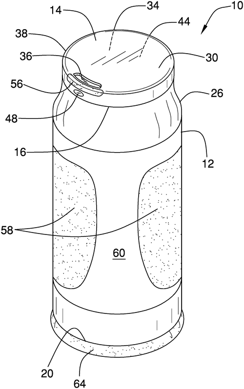
In the quest for spill-free beverage consumption, a new patent has emerged, outlining an innovative spill-resistant beverage container assembly. This invention comprises a cup and a lid designed to complement the top of the cup, providing a sealable closure. The lid features a sidewall extending between an upper plate and a lower plate, creating an interior space. An aperture is strategically positioned near the lid's circumference. What sets this invention apart is the inclusion of a detection and access module, which is coupled to the lid and positioned within the interior space. This module is programmed to sense motion near the aperture. When motion is detected, the module adjusts the lid to open the aperture, creating an access point for sipping the beverage within the cup. Although the concept of a spill-resistant beverage container assembly sounds promising, it is essential to consider the practicality of such an invention. Several competitors already offer spill-proof lids for cups, which are widely available and cost-effective. Therefore, the patent's realization as a marketable product may face challenges in standing out from existing offerings. However, the incorporation of motion-detecting technology in a beverage container raises intriguing possibilities for other applications. Imagine a lid that automatically opens when someone approaches, allowing them to drink hands-free. This could be useful in settings like hospitals or during sports activities, where convenience and hygiene are essential. In conclusion, while the spill-resistant beverage container assembly patent presents an interesting concept, its prospects as a commercially successful product remain uncertain. The market is already saturated with similar solutions, and it will require further innovation and added features to distinguish itself. Nevertheless, the technology behind the motion-detection module holds potential for wider applications. What other creative uses can you imagine for a beverage container with automatic access based on motion detection? Share your thoughts in the comments below!
The spill resistant beverage container assembly includes a cup and lid that are complementary to a top of the cup. The lid has a sidewall that is coupled to and extends between an upper plate and lower plate to define an interior space. An aperture is positioned in the lid proximate to a circumference of the lid. A detection and access module is attached to the lid, and is configured to detect motion in proximity to the aperture, positioning the detection and access module so that it opens the aperture so that beverages can be sipped from within the cup.
US Patent 11835368
****
Temperature Measuring Device and Method Calculate Second Reference Area, Third Temperature Measuring Area and Fourth Temperature Measuring Area
What is this invention?
Temperature measuring device and temperature measuring method
A temperature measuring device was made,
To measure the temp with a grade,
The processing module calculated areas two and four,
And the first detected value of the test subject it bore.
With this method from start to end we were saved!
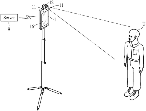
The latest patent application from XYZ Corporation reveals an intriguing temperature measuring device and method. This device, if it becomes a reality, could have various applications in industries such as healthcare, engineering, and manufacturing. The device consists of a processing module, a first image capturing module, and a second image capturing module. The processing module calculates different areas of temperature measurement based on the captured image information. By comparing the reference and temperature measuring areas of two image frames, the device determines the temperature values of different regions. The obtained temperature values can provide valuable insights into the thermal characteristics of a particular subject. Although the patent application does not explicitly mention the device's potential uses, one can envision several possibilities. In healthcare, for instance, this technology could be deployed in non-contact temperature measurement devices, providing a safer and more hygienic alternative to traditional thermometers. In engineering and manufacturing, it could aid in identifying hotspots in machinery or monitoring the temperature of various components during production. Competing products in the market, such as infrared thermometers and thermal imaging cameras, already offer similar functionalities. However, the novel approach described in this patent application may bring some distinctive advantages, such as enhanced accuracy or a more compact form factor. While this patent application holds promise, it's important to remember that not all inventions described in patents materialize into actual products. Obstacles like technical limitations, manufacturing feasibility, or market demand can hinder their development. Therefore, it remains to be seen if this temperature measuring device will make its way into the hands of consumers. What potential applications do you see for this innovative temperature measuring technology? Share your thoughts in the comments below!
A temperature measuring device and a temperature measuring method are provided. The temperature measuring device includes a processing module, a first image capturing module and a second image capturing module. The processing module calculates a second reference area, a third temperature measuring area and a fourth temperature measuring area of a second image information according to a first reference area, a first temperature measuring area and a second temperature measuring area of a first image information, respectively. The processing module obtains the first detected temperature value of the test subject in the third Temperature Measuring Area.
US Patent 11835389
****
New Pressure Sensor Is Protected From Environmental Conditions
What is this invention?
Sensors for pressure, forces, and couples
A pressure sensor that can detect
Forces in three directions, it's correct;
It also measures torque,
And its structure won't corrode--
Its behavior is hard to neglect!
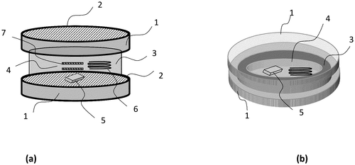
In a recent patent application, an innovative pressure sensor has been described that aims to revolutionize the field of force and torque measurement. The sensor, designed for multi-directional force and torque detection, capitalizes on the changes in reactive or mixed impedances when different forces and pressures are applied to its structure. The standout feature of this sensor lies in its closed and watertight space, ensuring that the device remains unaffected by varying environmental conditions. This robustness is a crucial advantage, as traditional pressure sensors often struggle to maintain accuracy and reliability in different settings. The potential uses for this invention are numerous. For instance, in automotive industries, it could be utilized to enhance safety features by providing real-time force and torque measurements, enabling smarter and more responsive control systems. In the field of robotics, such a sensor could help improve gripping and manipulation capabilities, ensuring greater precision and adaptability in various applications. While the patent application showcases an ingenious concept, it is important to note that not all inventions described in patents become actual products. Many technical and commercial challenges must be navigated before an innovation makes its way into the consumer market. Competitors with existing force and torque sensors may also pose stiff competition. Considering these factors, it would be interesting to hear from readers - do you think this pressure sensor has the potential to disrupt the force and torque measurement industry? How do you envision this technology being utilized in practical applications? Share your thoughts in the comments below.
The invention relates to a pressure sensor, which can be used to measure forces after one to three directions, normal to the sensor plane and tangential to the sensor plane. The sensor also has the ability to detect torques. The structure of the sensor is based on the variation of reactive or mixed impedances when applying normal forces or pressure and/or tangential forces or torques on the sensor structure. This makes it difficult for environmental conditions to affect the behavior of the sensor.
US Patent 11835401
****
Tension Sensors: A New Way to Monitor Strain
What is this invention?
Thinline towed array tension sensor
A tension sensor so fine and grand,
Is quite a complex piece of land.
It has two strain gages that will astound,
Aligned to the tab's longitudinal sound.
The Wheatstone bridge is on each side bound!
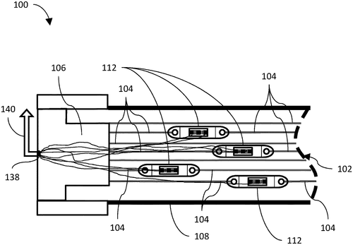
A recent patent for a tension sensor has caught the attention of tech enthusiasts, promising a breakthrough in measuring tension with precision. The sensor consists of a planar tab with strain gauges attached to both sides, along with a Wheatstone bridge wiring configuration. The innovation lies in the design of the strain gauges, which have a tension grid aligned to the longitudinal axis of the tab and a cross-tension grid perpendicular to it. When wired in a Wheatstone bridge, the tension grid and cross-tension grid of the first strain gauge form one side, while the tension grid and cross-tension grid of the second strain gauge make up the other side. The potential applications for this technology are vast. Industries that rely on accurate tension measurements, such as construction, aerospace, and robotics, could benefit from this sensor. For example, in construction, the sensor could be used to ensure the proper tension in cables and support structures, leading to increased safety and efficiency. Although the patent provides an intriguing concept, it is essential to recognize that having a patent does not guarantee a product will be developed. Many patents never materialize into actual consumer products. In this case, it would be interesting to see if any companies in the tension monitoring field will take up this innovation and incorporate it into their products. Competitors in the market already offer tension sensors, but this particular design has the potential to deliver improved accuracy and reliability due to its unique strain gauge configuration. It's worth pondering whether this tension sensor patent will pave the way for a new era of precise tension measurement. Can you envision any other industries or applications where this technology could revolutionize existing practices? Share your thoughts in the comments below.
A tension sensor includes a planar tab having a first and second side, first and second end sections, and an aperture through each of the end sections. A first strain gage is attached to the first side of the tab. The first strain gage has a tension grid aligned to a longitudinal axis of the tab and a cross-tension grid perpendicular to the tension grid. A second strain gage is attached to the second side of the tab. The second strain gage has a tension grid aligned to the longitudinal axis of the tab and a cross-tension grid perpendicular to the tension grid. The first strain gage and second strain gage are wired in a Wheatstone bridge in which the tension grid and cross-tension grid form one side and each side of this bridge forms another side.
US Patent 11835404
****
Wireless Sensor Data Provides Insight Into Tire Conditions
What is this invention?
Sensor assemblies and systems for monitoring a dynamic object
A sensor assembly and system was made,
To monitor and transmit data relayed.
The housing displays the indicia,
Which helps with electrical components' area.
It receives data to show conditions that fade!
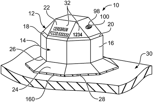
Sensor assemblies and systems have always played a crucial role in monitoring various operating parameters of dynamic articles. However, a new patent has recently caught our attention with its innovative approach to sensor housing and data transmission. According to the patent description, this new sensor assembly comprises a housing that houses an electrical sensor device. The primary purpose of this housing is to protect the sensor device while providing relevant display indicia related to the sensor assembly. The electrical sensor device is equipped with components necessary for monitoring and wirelessly transmitting desired data regarding the operating conditions of the dynamic article it is attached to. One of the potential applications of this invention is in the automotive industry, specifically in vehicle tires. When the sensor assembly is attached to a vehicle tire, it can monitor and transmit data on various parameters such as outside diameter, tread depth, pressure, radial load, vehicle camber, toe alignment variations, and even tire/vehicle location. This data can be wirelessly received by an external receiver to determine the current operating conditions of the tire. While this patent presents an intriguing concept, it is important to note that being granted a patent does not necessarily guarantee that a product will ever be created based on that patent. Many factors come into play, including technical feasibility, market demand, and manufacturing costs. Additionally, there are already existing products in the market that provide similar functionalities, such as tire pressure monitoring systems (TPMS). It will be interesting to see how this invention evolves in the future. Will it be developed into a commercially viable product? Can it provide enhanced accuracy and additional features compared to existing solutions? What other industries could benefit from this innovative sensor assembly design? We invite you to share your thoughts and speculations in the comments below.
This text describes a sensor assembly and system that can be used to monitor and transmit data relating to operating parameters/conditions of a dynamic article, such as a tire. The housing may include display indicia relating to the sensor assembly, and the electrical components within the sensor assembly are useful for monitoring and transmitting desired data. The receiver external from the dynamic article receives this data to determine various operating conditions.
US Patent 11835421
CANON KABUSHIKI KAISHA
Calculating an Inspection Target's Position or Angle with Precise Accuracy
What is this invention?
Method for calculating position or angle of inspection target, storage medium, apparatus, and system
There's a method for calculations
For an angle or position estimations
It uses sine and cosines
To acquire amplitudes finesse
And the offset error will give you revelations
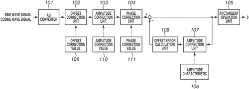
In a recent patent filing by Canon Kabushiki Kaisha, a method for calculating the position or angle of an inspection target is described using a sine wave signal and a cosine wave signal derived from an encoder or a laser interferometer. The innovation involves acquiring the temporary movement speed of the inspection target, calculating an amplitude correction value based on the relationship between the movement speed and the amplitudes of the sine and cosine wave signals, and then using this correction value to adjust the amplitudes of the signals. By analyzing the resulting Lissajous waveform and calculating the offset error, the position or angle of the inspection target can be determined. This patent, if implemented successfully, could have significant implications for various industries that rely on accurate position or angle calculations during inspections. For example, in manufacturing, such a method could enhance the accuracy and reliability of quality control processes. It also has the potential to improve the efficiency of robotic systems in areas like assembly lines or material handling. While this patent shows promising potential, it is important to keep in mind that not all innovations described in patents make it to commercial products. Canon Kabushiki Kaisha would need to invest in further development, testing, and validation to determine the feasibility and practicality of this method. Moreover, it is essential to consider existing competitor products that might already offer similar capabilities. In conclusion, Canon Kabushiki Kaisha's patent presents an intriguing idea for accurately calculating the position or angle of an inspection target. The proposed method, if realized, could find applications in various industries and enhance precision in critical processes. However, whether this invention will make its way into practical use remains to be seen. What industries do you think would benefit the most from the implementation of this method? Share your thoughts in the comments below.
The method for calculating a position or an angle of an inspection target based on a sine wave signal and a cosine wave signal output from an encoder or a laser interferometer includes acquiring a temporary movement speed of the inspection target, calculating an amplitude correction value corresponding to the temporary movement speed using information representing a relationship between a movement speed of the inspection target and amplitudes of the sine wave signal and the cosine wave signal acquired in advance, correcting the amplitudes of the sine wave signal and the cosine wave signal using the amplitude correction value, and calculating an offset error in a Lissajous waveform using the sine wave signal and the cosine wave signalthe amplitudes of which are corrected with the amplitude correction value. The position or angle of the inspection target can then be calculated based on this offset error.
US Patent 11835370
CANON KABUSHIKI KAISHA
Pulse-Powered Photoelectric Conversion Device Keeps Counting
What is this invention?
Photoelectric conversion device, imaging system, light detection system, and mobile body
A photoelectric conversion device was found,
It had an avalanche photodiode around,
A pulse count unit to keep track of the sound,
And a time count unit that kept spinning around.
The threshold calculationunit made sure no one would frown,
For it calculated the threshold value with precision and not by chance in town!
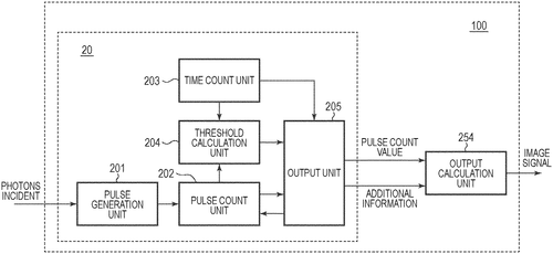
Canon Unveils Innovative Photoelectric Conversion DeviceCa. non Kabushiki Kaisha has recently filed a patent for a groundbreaking photoelectric conversion device that could potentially revolutionize the photography industry. The device, described in the patent as an "avalanche photodiode", offers a unique set of features that sets it apart from its competitors. One of the key features of this device is its pulse generation unit, which efficiently converts the output from the avalanche photodiode into a pulse signal. This ensures accurate conversion and representation of the captured image. In addition, the pulse count unit provides a pulse count value, allowing for precise measurement of the pulse signal. What sets this device apart is the inclusion of a time count unit and a threshold calculation unit. These components work together to enhance the output unit's functionality: when the pulse count value surpasses a specific threshold value, the counting is halted, and the time count value is outputted. This unique characteristic enables users to gain insights into the precise timing of specific events or actions, offering potential applications in various industries, such as sports photography or scientific research. While this patent showcases Canon's innovative approach to photoelectric conversion, it is important to note that not all patented inventions make their way into commercial products. Although there is significant potential for this device, it remains to be seen whether Canon will develop it further and incorporate it into their future camera offerings. It is worth considering how this new technology could disrupt the market and possibly challenge existing photoelectric conversion devices. How do you envision this device being used in real-world applications? Let us know your thoughts in the comments below. Note: This review is based on a patent filed by Canon Kabushiki Kaisha and does not guarantee the development or availability of this device in the market.
The photoelectric conversion device according to an embodiment of the present disclosure includes an avalanche photodiode, a pulse generation unit that converts an output from the avalanche photodiode into a pulse signal, a pulse count unit that counts the pulse signal and outputs a pulse count value, a time count unit that outputs a time count value indicating a time from the start of operation of the pulse generation unit, an output unit that, when the pulse count value does not exceed a threshold value, outputs the pulse count value, and when the pulse count value exceeds the threshold value, ends counting in the Pulse Count Unit and outputs the timecountvalue at t he tim e o f t he pulse cOUNT v alue ex ce pting th e threshold. Threshold calculationunit calculates t hethresholdv alue usin gt his tim ecount v alue.
US Patent 11835386
CANON KABUSHIKI KAISHA
See the world in a new way with terahertz technology
What is this invention?
Terahertz wave camera system and method for controlling terahertz wave camera system
A system was made with a plan,
First and second transmission units ran.
The detection unit would detect,
Reflected terahertz waves it did expect.
And the control unit set conditions based on what it had seen!
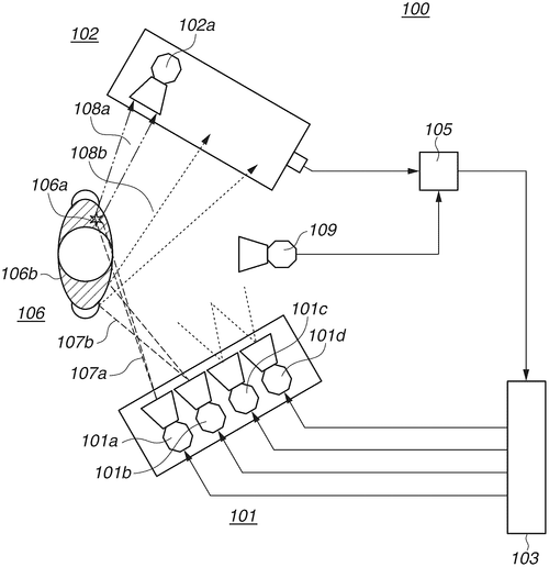
In a recent patent filing, Canon Kabushiki Kaisha has revealed a system that utilizes terahertz waves to capture images. The system consists of a first transmission unit that emits a terahertz wave, a second transmission unit situated in a different position, a detection unit that captures the reflected terahertz waves from an object, and a control unit that adjusts the operations of the transmission units based on the captured data. While the concept of using terahertz waves for imaging is intriguing, it is important to note that this is just a patent filing and not a confirmed product. Terahertz imaging technology has shown potential in various applications, including medical imaging and security scans. However, Canon faces competition from other companies actively working on similar technologies, such as Terasense and Teraview. One possible use for this system could be in the field of security. By utilizing terahertz waves, security personnel could potentially identify concealed weapons or contraband without needing physical contact, offering a non-invasive and efficient screening process. Despite the promising aspects of the patent, it is essential to consider the practicality of implementing such a system. Terahertz imaging has faced challenges in terms of cost, range limitations, and image quality. Achieving a balance between these factors will be crucial for Canon to turn this concept into a feasible product. As we wait to see if Canon will develop this intriguing invention into a marketable product, let us ponder how terahertz imaging could revolutionize various industries. What potential applications do you envision for this technology? Let us know in the comments below.
The system includes a first transmission unit that emits a first terahertz wave, a second transmission unit that is disposed at a position different from the first transmission unit and configured to emit a second terahertz wave, and a detection unit that detects at least one of a first reflected terahertz wave that is part of the first terahertz wave reflected from an object, or a second reflected terahertz wave that is part of the second terahertz wave reflected from the object. The image data based on the detected terahertz waves is outputted by the detection unit. The first control unit controls at least one of an operation of the first transmission unit or an operation of the second transmission unit under a condition set based on the image data.
US Patent 11835452
CANON KABUSHIKI KAISHA
New Detection Apparatus Detects Marks With Precise Accuracy
What is this invention?
Detection apparatus, detection method, exposure apparatus, exposure system, and article manufacturing method
A detection optical system was found,
That irradiated light on the ground.
The processor then did detect,
The mark it did select,
And a correction value was sound.
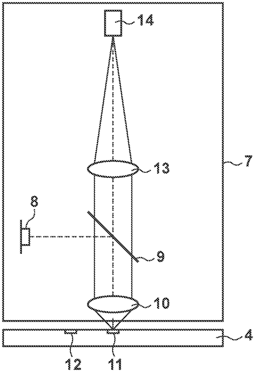
Canon, the renowned multinational corporation specializing in imaging and optical products, has recently filed a patent for a detection apparatus that could potentially revolutionize mark detection on substrates. The patent outlines a device consisting of a detection optical system, which illuminates a mark on a substrate and captures an image of it, and a processor that analyzes the image to perform a detection process. The primary innovation of this detection apparatus lies in its ability to accurately determine the position of the mark within the observation field of the detection optical system. Through the use of detection values, the processor calculates the precise coordinates of the mark, enabling efficient analysis and subsequent actions. Furthermore, this patent introduces the concept of subregions within the observation field. By identifying which subregion the mark is located in, the detection apparatus can apply specific correction values to improve the accuracy of the detection process. This thoughtful adjustment methodology ensures that potential errors in detection caused by variations in subregion characteristics are effectively minimized. While the patent certainly demonstrates an intriguing advancement in mark detection technology, it is important to note that being granted a patent does not necessarily guarantee that a product will be developed or brought to market. Other companies in the imaging industry, such as Nikon and Sony, have also explored similar technologies, but it remains to be seen whether they will be able to turn these innovations into commercially viable products. In terms of potential applications, the detection apparatus could find utility in various industries, including manufacturing, quality control, and even forensic investigations. Its ability to swiftly and accurately detect marks on different substrates could streamline processes and improve overall efficiency. As an inquisitive writer, I wonder how this patent aligns with Canon's current product roadmap. Will they choose to fully develop this detection apparatus, or might they focus their efforts on alternative technologies? I invite you, dear readers, to share your thoughts and speculations in the comments below.
The detection apparatus includes a detection optical system that irradiates light on the mark on the substrate and detects an image of the mark. The processor then performs a detection process of the mark based on the image of the mark, finds a subregion in which the mark is located among a plurality of subregions in the observation field, and corrects the detection value based on a correction value corresponding to the found subregion among correction values predetermined for the plurality of subregions.
US Patent 11835470
Dell Products L. P.
PCB Signal Loss Compensation Ensures Quality Broadcasts
What is this invention?
Compensating for signal loss at a printed circuit board
A communication system was in need,
For signal loss it did plead.
The expected losses were found at two freqs,
And the rate of change was next.
Gain compensation then went to effect
To keep a good connection direct!
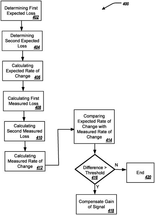
If you've ever experienced signal loss or weak connectivity while using your electronic devices, Dell may have a solution for you. A recent patent application by Dell Products L. P. describes a technology that aims to compensate for signal loss and enhance the strength of transmitted signals. The patent details a method that involves several steps to address signal loss. First, the expected loss at different frequencies is determined, followed by the calculation of the expected rate of change of this loss. Then, the measured loss of signals at various frequencies is calculated, and the measured rate of change is determined. Finally, the measured rate of change is compared with the expected rate of change, and the signal gain is adjusted accordingly. While the patent application provides an intriguing idea for improving signal strength, it is crucial to note that patents don't always result in real-world products. It's common for companies, including Dell's competitors, to file patents that never see the light of day as consumer products. Therefore, it's vital to approach this innovation with a dose of skepticism. If developed into a physical product, this technology could have a multitude of potential applications. It could enhance the performance of wireless devices such as smartphones, laptops, and tablets. It may also find use in other areas that rely on strong signal transmission, like Internet of Things (IoT) devices, automotive communication systems, or even satellite communications. It remains to be seen whether Dell will eventually implement this technology in their products. In the meantime, it's worth pondering the possibilities this innovation presents. How would your experience using everyday devices be improved if signal loss was effectively compensated? Share your thoughts in the comments below. Sources: Dell Products L. P.
This document describes a method for compensating for signal loss in a communication system. First, an expected loss at a first frequency and an expected loss at a second frequency are determined based on the receiver's capabilities. Next, an expected rate of change of signal loss between the first and the second frequencies is calculated based on these losses. Finally, a gain of the signal transmitted from the transmitter to the receiver is compensated based on this measured rate of change.
US Patent 11835576
Dell Products L. P.
Cable Assembly with Multiple Breakouts Provides Superior Communications
What is this invention?
Two-by-two cable assembly
A cable assembly with two ends,
The first had a breakout of friends.
The second shared one more,
With the third and fourth floor,
So the channels could all make amends.
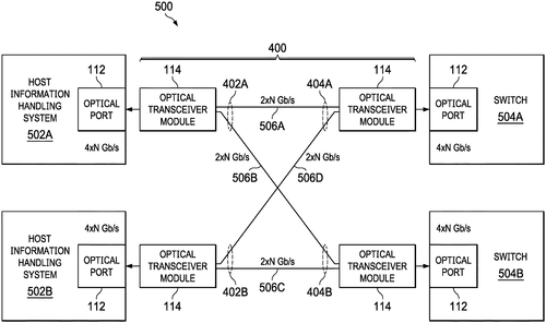
Innovation in the tech industry never seems to slow down, with new patents and inventions constantly pushing the boundaries of what's possible. Today, we take a closer look at Dell Products L. P.'s latest patent, which introduces us to a cable assembly that aims to revolutionize communications channels. The cable assembly described in the patent consists of a first end and a second end, each containing multiple breakout points. These breakout points, in turn, comprise a variety of conduits implementing communications channels. What sets this invention apart is the strategic arrangement of these channels, allowing for seamless sharing and transmission of data. Upon thorough examination of the patent, it becomes clear that this cable assembly intends to optimize communication efficiency by sharing channels between different breakouts. For example, the first breakout shares a communications channel with the third breakout, while the second breakout shares channels with both the third and fourth breakouts. This clever arrangement allows for enhanced data transfer capabilities, potentially leading to faster and more reliable connections. While the patent description outlines many technical specifics, it remains to be seen how this cable assembly could be put to practical use. The tech market is filled with similar products, such as HDMI cables and USB-C connectors, which already handle various data transmission needs. To successfully compete against these established solutions, Dell Products L. P. must demonstrate not only the theoretical potential of its patent but also provide a compelling use case that outshines existing options. That being said, there is undoubtedly potential for this cable assembly to find its place in various industries where efficient communication is critical. One can imagine applications in fields such as telecommunications, data centers, and multimedia production, where the need for high-speed, reliable connections is paramount. As with any patented invention, we must remember that not every idea becomes a commercial reality. It will be interesting to follow Dell Products L. P.'s journey with this cable assembly and see if it manages to overcome the challenges of bringing a new product to market. Now, we turn the question over to you, dear readers. What do you think about Dell Products L. P.'s cable assembly patent? Do you see a need for such an innovation, or do you believe existing products already fulfill the demand? Share your thoughts and opinions in the comments section below.
This cable assembly includes a first end and a second end. The first end includes a first breakout including a plurality of transmissive conduits implementing a plurality of communications channels, and the second end includes a fourth breakout including a plurality of conduits implementing a plurality of communications channels. Communication channels of the first breakout, second breakout, third breakout, and fourth breakout are arranged such that the first breakout shares one communication channel with the third breakout, the first breakup shares another communication channel with the fourth break-out, the second breakup shares yet another communication channel with the third break-out, and finally, the fourth breakup shares yet another communication channel with the fourth break-out.
US Patent 11835781
Dell Products L. P.
Configurable Component Receptacle Provides Flexibility for Information Handling System
What is this invention?
Configurable component receptacle for use with information handling systems
A configurable component receptacle,
With a holder and flexible portion.
It can be in either horizontal or pivoted;
Configured from one piece material-fitted.
Attached to the frame of an info handling system -
Providing many options for them!
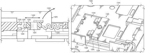
Dell's Latest Patent Paves the Way for Customizable Information Handling SystemsDe. ll Products L. P. is making headlines once again with its new patent for a configurable component receptacle. This innovative invention allows users to easily customize an information handling system by providing a holder portion and a flexible portion. The holder portion, made from a single piece of material, is designed to hold various components of an information handling system. What sets this patent apart is the flexibility of the receptacle, which enables it to be configured in both a horizontal and pivoted position. This means that users can easily adjust their system to fit their specific needs and preferences. In the competitive market of information handling systems, where options and configurations seem endless, Dell's patent offers a promising solution. With this invention, users are no longer limited to a fixed setup or forced to purchase new hardware when their needs change. Instead, they can simply adjust the holder portion according to their desired configuration. Imagine having the ability to effortlessly switch between a horizontal configuration for standard use and a pivoted configuration for special projects or collaborations. This patent opens up a world of possibilities for information handling systems, as it empowers users to customize their devices based on their unique requirements. While this patent showcases Dell's commitment to innovation, it's important to acknowledge that not all patented inventions make it into commercial products. Oftentimes, patents are filed to protect intellectual property or as a strategic move against competitors. Therefore, it remains to be seen whether Dell will transform this patent into a tangible product that consumers can get their hands on. That being said, Dell's configurable component receptacle is undoubtedly a development that would intrigue tech enthusiasts and professionals alike. It addresses the ever-changing needs of users by providing a versatile solution to customization. As we wait for Dell's next move, one can't help but wonder how this patent might revolutionize the future of information handling systems. So, what are your thoughts on Dell's latest patent? Do you believe this invention has the potential to reshape the way we customize our devices? Share your opinions and insights in the comments below.
The configurable component receptacle includes a holder portion and a flexible portion. The flexible portion enables the holder portion of the configurable component receptacle to be in a horizontal configuration and a pivoted configuration. The holder portion and the flexible portion are configured from a single piece of material. The configurable component receptacle is attached to a frame of an information handling system, enabling configuration of the information handling system with a plurality of component options.
US Patent 11836008
Dell Products L. P.
Detachable Keyboard Case for Multi-Form Factor IHS
What is this invention?
Foldable case for a multi-form factor information handling system (IHS) with a detachable keyboard
A folio case was quite unique
It had magnets on each side to seek.
Coupled at the top and bottom,
For easy folding it had no problem,
This arrangement made it small and neat!
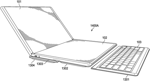
Dell Products L. P. has recently patented an intriguing concept: a foldable case for a multi-form factor IHS (Intelligent Human System) with a detachable keyboard. The case, described as a folio, consists of three panels, each equipped with left-side and right-side magnets. The panels are cleverly designed to fold and connect, creating a protective and versatile case for the device. Upon reading the patent, one can't help but be reminded of the growing trend of foldable devices such as smartphones and tablets. Industry giants like Samsung and Huawei have already launched their respective foldable smartphones, showcasing the potential of this form factor. With Dell's foray into foldable cases, it is evident that they are keen to explore the expanding market of adaptable devices. The patent describes the detachable keyboard as a unique feature, which indicates Dell's focus on productivity and versatility. The ability to easily switch between typing on a physical keyboard and utilizing the device in tablet mode could be incredibly useful for professionals on the go. While the concept sounds intriguing on paper, it is crucial to keep in mind that a patent does not guarantee a product will come to fruition. Many patents are filed as a means of protecting intellectual property, and not all end up being developed into tangible products. Furthermore, the foldable market itself is still relatively nascent, with various challenges in terms of durability and user experience. It would be interesting to see how Dell tackles these challenges and whether they are able to bring this concept to life. Will we witness a foldable IHS with a detachable keyboard, or will this patent remain nothing more than an idea? Share your thoughts in the comments below.
The folio case described herein includes a first panel with left-side and right-side magnets, a second panel with left-side and right-side magnets, and a third panel with left-side and right-side magnets. The first panel is coupled to the second panel at the top edge and the bottom edge, while the third panel is coupled to the second panel at the top edge and the bottom edge. This arrangement allows for easy folding of the folio case so that it can be stored or transported in a compact manner.
US Patent 11836012
Dell Products L. P.
modular compute chassis, modular processing unit, and air mover units - remove your equipment with ease
What is this invention?
Modular removable air mover for dual access
A modular compute chassis was found,
With a processing unit on the ground.
It could remove from the front,
In a direction that's blunt,
And the air mover unit at its rearward bound.
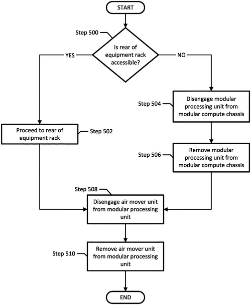
Dell Products L. P. has recently filed a patent for an intriguing piece of equipment rack technology. The patent describes an equipment rack that boasts a modular compute chassis, a modular processing unit, and an air mover unit. What sets this invention apart is its innovative design that allows for easy removal of the processing unit from the front of the compute chassis, as well as the air mover unit from the rear of the processing unit. While the details provided in the patent are concise, it leaves us wondering about the potential applications and advantages this technology could bring. The ability to remove the processing unit from the front and the air mover unit from the rear could potentially make maintenance and upgrades more efficient. This design might also allow for easier customization and scalability, giving users the flexibility to adapt the equipment rack to their specific needs. Competitors in the market, such as Hewlett Packard Enterprise and Cisco Systems, already offer similar equipment rack solutions. However, Dell's patent hints at a unique approach that could potentially remedy certain challenges faced by their competitors' products. As exciting as this patent sounds, it's important to note that many patented inventions never make it to the production stage. We're left wondering if Dell will actually bring this concept to life and turn it into a practical and marketable product. What do you think of Dell's modular equipment rack? Do you believe the ability to remove the processing unit and air mover unit from different sides of the chassis could bring significant advantages? Let us know your thoughts in the comments below!
The equipment rack includes a modular compute chassis, a modular processing unit located in the modular compute chassis and where the modular processing unit is configured to remove from the front of the modular compute chassis in a frontward direction, relative to the front side of the modular compute chassis. The air mover unit is located in the modular processing unit and is configured to remove from a rear side of the modular processing unit in a rearward direction, relative to the front side of modular compute chassis.
US Patent 11836019
Canon Kabushiki Kaisha
New Polygon Mirror with Improved Height Accuracy
What is this invention?
Polygon mirror, optical deflector, optical scanning device, and image forming apparatus
A polygon mirror included a resin,
It had two surfaces and an inner join.
The first segment was tall,
But the second one did fall,
Depressed from its reference to the loin.
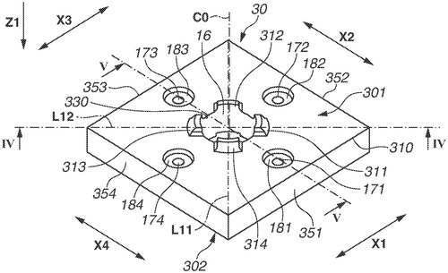
Canon Kabushiki Kaisha has recently filed a patent for a new polygon mirror that showcases their continued commitment to optical technology. The patent describes a polygon mirror that is comprised of a resin member with multiple surfaces and an inner surface surrounding a through hole. The outer surfaces join the first and second surfaces, creating a unique design. One noteworthy feature of this polygon mirror is the inclusion of a projection on the first surface, which forms the inner surface and extends towards the opposite side of the second surface. Additionally, the second surface includes a depressed portion that is distant from the outer surfaces and angles towards the first surface. While this patent demonstrates Canon's dedication to pushing the boundaries of optical technology, it remains to be seen if this invention will ever make it to the market. As with many patents, the road from concept to commercialization can be long and uncertain. Canon needs to carefully consider the demand and feasibility of incorporating this new design into their products. In terms of potential applications, this innovative polygon mirror could have implications in various industries, such as laser technology, spectroscopy, and optical communications. By improving the precision and functionality of polygon mirrors, Canon could potentially revolutionize these sectors. It's worth noting that Canon will face competition from other established players in the market, such as Nikon and Sony. These companies have their own research and development teams constantly working on new technologies, ensuring a competitive landscape for Canon's polygon mirrors. The question remains: Will Canon be able to transform this patented design into a commercially viable product? How would you envision this technology being utilized in practical applications? Share your thoughts and predictions in the comments below.
A polygon mirror includes a resin member, first and second surfaces, an inner surface joining the first and second surfaces to surround a through hole extending from the first to the second surface, and outer surfaces joining the first and second surfaces. A first segment between the first surface and the outer surfaces is defined as a first reference of a height in a direction from a second segment between the second surface and the outer surfaces to the first segment. The first surface includes a projection that forms the inner surface and projects from the first reference toward a side opposite to the second surface. The depressed portion distant from the outer surfaces is depressed from the second reference towardthe Firstsurface.
US Patent 11835714
Canon Kabushiki Kaisha
Toner Classification Apparatus Provides Precise Toner Production
What is this invention?
Toner classification apparatus and toner production method
There was a toner classification apparatus,
Which had a vane A that did surpass
Vane B in length, so they'd be
In the right relationship you see.
A production method it does amass!
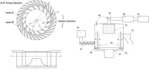
In a recent patent application, Canon Kabushiki Kaisha unveils an innovative toner classification apparatus. This apparatus features a classification rotor with two vanes - vane A and vane B. Vane A extends from the rotation center direction of the classification rotor to its outer circumference, while vane B is longer than vane A. The arrangement of vane A and vane B is designed to meet a predetermined relationship. Additionally, the patent describes a toner production method that involves the classification of particles using this unique toner classification apparatus. This invention by Canon shows promise in improving toner classification processes. Efficient and accurate classification of toner particles is crucial in the production of high-quality prints. By utilizing a classification rotor with carefully positioned vanes, the apparatus could optimize the separation of different toner particles based on their sizes and characteristics. This could lead to more reliable and consistent toner production, resulting in enhanced print quality. In a competitive market, Canon faces contenders like Xerox and HP, who have their own toner classification technologies. However, Canon's proposed apparatus, with its novel vane configuration, demonstrates their commitment to advancing print technology. While this patent showcases an exciting innovation in toner classification, it's important to note that not all filed patents necessarily make it to market as actual products. The implementation feasibility, cost-effectiveness, and demand are crucial factors that need to be taken into consideration. Considering the potential applications, could this toner classification apparatus by Canon revolutionize the printing industry? How would improved toner classification impact daily printing needs? Share your thoughts in the comments below.
The text describes a toner classification apparatus and a toner production method. The apparatus includes a classification rotor having a vane A which extends from a rotation center direction of the classification rotor to an outer circumference direction thereof and a vane B having a length longer than that of the vane A. The vane A, vane B, and the rotation center direction are disposed so as to satisfy a predetermined relationship. In addition, the toner production method includes a classification step of carrying out a classification process on particles to be classified by using the apparatus.
US Patent 11835875
Canon Kabushiki Kaisha
Removable and Easy-to-Mount UFP Collection Filter Keeps Duct Unit in a State of Holding
What is this invention?
Image forming apparatus having removable duct and filter
A duct unit with a UFP filter,
Made it easy to collect ultrafine particles.
It was removable and mounted easily,
So the filter could be exchanged readily.
Making maintenance of the duct a breeze!
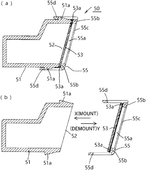
Canon Kabushiki Kaisha has recently filed a patent that could potentially revolutionize the way printers function. According to the patent description, the company aims to tackle the issue of ultrafine particles (UFP) that are released during the printing process. These particles can be harmful to both the environment and human health. Canon's innovation involves the installation of an UFP collecting filter that is easily replaceable, allowing for convenient removal and exchange. This invention addresses a significant concern in the printing industry, as current printers often lack efficient mechanisms to deal with UFP emissions. The inclusion of a removable UFP collecting filter can potentially minimize pollution and improve air quality in office environments. Although the concept outlined in the patent holds promise, it's important to consider the feasibility of its implementation. Currently, Canon has not announced any plans for the production or release of a printer incorporating this technology. Moreover, it would be interesting to examine how this patent compares to existing solutions or competitive products in the market, such as specialized air purifiers designed for printers. Expanding our perspective, the potential applications of this technology could go beyond the printing realm. Imagine if this UFP collecting filter could be integrated into other devices that emit harmful particles, such as industrial machinery, to create a cleaner and healthier workspace. In the comments below, we would like to hear your thoughts on this patent. Do you think the industry could benefit from such a technology? Can you envision any other practical applications for UFP collecting filters? Let us know!
This text describes a system for collecting ultrafine particles. The system includes a duct unit that is removable and easily mounted to a duct, and an ultrafine particle (UFP) collecting filter between transfer and fixing. This allows the filter to be easily exchanged, which makes it easier to maintain the duct unit.
US Patent 11835876
Canon Kabushiki Kaisha
Rotatable Polygon Mirrors with Higher Top Surface Protrusion Points
What is this invention?
Rotatable polygon mirror, optical deflecting device, scanning optical device, and image forming apparatus
A polygon mirror rotatable,
With protrusion portions annular.
The heights differ in the axis direction,
To stack them with precision.
Engaging walls for a strong connection!
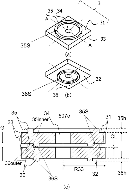
Canon Kabushiki Kaisha, a leading company in imaging and optical products, has recently filed a patent for a rotatable polygon mirror. This innovative mirror consists of multiple reflecting surfaces and is designed with first and second protrusion portions in an annular shape. These protrusion portions are positioned on opposite ends, protruding inversely to each other in the rotational axis direction. One notable feature of this polygon mirror is the difference in height between the top surface portions of the first and second protrusion portions. The top surface of the first protrusion portion, measured from the first surface, is higher than the top surface of the second protrusion portion, measured from the second surface, with respect to the rotational axis direction. The patent also highlights the interaction between these protrusion portions when multiple mirrors are stacked in the rotational axis direction. In this configuration, the inner peripheral wall of the first protrusion portion and the outer peripheral wall of the second protrusion portion engage with each other, ensuring stability and precision in the rotations. While this patent presents an interesting development in mirror technology, it is important to remember that patents do not necessarily guarantee the creation of an actual product. Canon is a reputable company known for pushing the boundaries of imaging, but it remains to be seen if this particular invention will be developed into a market-ready product. If realized, this rotatable polygon mirror could have potential applications in various fields, such as laser scanning systems or optical communication devices. However, it's worth noting that there are already competing products on the market that serve similar purposes. What are your thoughts on this patent? Do you see any specific industries or applications where this rotatable polygon mirror could make a significant impact? Share your opinions in the comments below.
A rotatable polygon mirror includes a plurality of reflecting surfaces, first and second protrusion portions with an annular shape, provided on the first and second surfaces and protruding inversely to each other in the rotational axis direction about a rotational axis of the rotatable polygon mirror. The height of the top surface portion of the first protrusion portion from the first surface is higher than that of the top surface portion of the second protrusion portion from the second surface with respect to the rotational axis direction. In a case that the rotatable polygon mirrors are stacked in the rotational axis direction, a wall of an inner peripheral side of the first protrusion portion and a wall of an outer peripheral side of the second protrusion portion are engaged with each other.
US Patent 11835880
Canon Kabushiki Kaisha
New image forming apparatus switches speed of polygon mirror for perfect printing
What is this invention?
Image forming apparatus with switched process speeds and resolutions
A scanning means with light source too,
Was used to irradiate an area view.
The polygon mirror was set in motion,
With a driving means for rotation.
The controller switched the speed it flew!
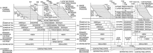
In a recent patent filed by Canon Kabushiki Kaisha, an intriguing image forming apparatus is described. This device includes a scanning mechanism with a light source, a polygon mirror, and a driving mechanism to control the rotation of the mirror. Alongside these components, the apparatus also features a photosensitive member, a developing mechanism, and a detecting mechanism to identify laser light emitted by the light source. The patent outlines a controller that effectively operates the apparatus, initiating a light emission operation that irradiates an area encompassing the image forming region of the photosensitive member with laser light. Moreover, the controller can execute a switching operation, altering the rotational speed of the polygon mirror from a first speed to a second speed, different from the initial speed. These operations are executed while the photosensitive member and the developing means are in contact and rotating, based on the detection results obtained by the detecting mechanism during the light emission operation. While this patent showcases Canon's innovative approach to image forming technology, it is important to acknowledge that not all patented inventions translate into commercially viable products. Canon faces competition from established brands producing similar image forming apparatuses, such as those offered by Epson and Hewlett-Packard. Additionally, the practical applications of this invention remain speculative and warrant further exploration. The image forming apparatus described in the patent could potentially have various use cases across industries. For instance, it could find utility in high-speed printing for businesses or be employed in advanced 3D imaging systems, revolutionizing the way we capture and reproduce complex visual data. As with any new technology, it is crucial to consider the real-world feasibility and market demand for such products. While this patent hints at a novel approach, it remains to be seen whether Canon will fully develop and release a tangible device based on this invention. What potential applications can you envision for this image forming apparatus? Share your thoughts in the comments below.
The text describes an image forming apparatus that includes a scanning means, a polygon mirror, and a driving means for rotating the polygon mirror. The scanning means is provided with a light source and is configured to irradiate an area including an image forming area of a photosensitive member with laser light. The controller controls the driving means to switch the rotational speed of the polyzon mirror from a first speed to a second speed different from the first speed. In addition, the controller controls the driving means to execute light emission operation in which an area including the image forming area of the photosensitive member is irradiated with laser light. Finally, based on detecting result of detection means in the light emission operation, the controller controls switching operation in which rotational speed of polygon mirror is switched from first speed to second speed.
US Patent 11835881
Micron Technology, Inc.
Hybrid Memory System Interface Allows for Block Level Storage I/O and Sub-Block Level Storage I/O
What is this invention?
Hybrid memory system interface
A hybrid memory system interface,
For many types of computing device;
It supports both block level and sub-block I/O,
So you can use it to go;
The present disclosure is really quite nice!

Micron Technology, Inc. has recently filed a patent for a hybrid memory system interface, which could potentially revolutionize the way computing systems interact with storage systems. This innovative interface aims to provide a more efficient and versatile input/output (I/O) access path between a processing resource and a storage system. One key feature of this hybrid interface is its ability to support both block level storage I/O access requests and sub-block level storage I/O access requests. This means that it can handle larger data transfers, as well as smaller, more specific data access. This flexibility could greatly improve data processing and retrieval speeds, making it a potentially valuable tool for various industries. While the patent application does not explicitly mention specific use cases, one can imagine a multitude of potential applications. For example, in the field of data analysis, this hybrid interface could provide faster access to large datasets, enabling more efficient processing and analysis. Similarly, in the realm of virtual reality and gaming, this technology could result in smoother gameplay experiences by quickly loading and rendering complex graphics and environments. Of course, it is important to note that a patent application does not guarantee that this technology will become a widely available product. Many factors come into play before an invention makes it into the market, such as feasibility, cost-effectiveness, and market demand. However, it is undeniably an intriguing concept that could potentially address some of the performance limitations faced by current storage system interfaces. In the realm of competitors, there are already established products in the market that offer similar functionalities. For instance, Intel's Optane Memory technology aims to accelerate storage performance by combining traditional solid-state drives (SSDs) with Intel's own memory technology. Samsung also offers its Z-NAND SSD, which boasts lower latency and higher performance compared to traditional NAND-based storage. It would be interesting to see how Micron's hybrid memory system interface would compare to these existing solutions. Overall, Micron Technology's patent for a hybrid memory system interface shows promise for enhancing computing system performance by improving storage I/O access. However, only time will tell if this technology will materialize into a practical product that can benefit a wide range of industries. What potential applications can you envision for a hybrid interface that supports both block level and sub-block level storage I/O access requests? Share your thoughts in the comments below.
The present disclosure includes apparatuses and methods related to a hybrid memory system interface. An example computing system includes a processing resource and a storage system coupled to the processing resource via a hybrid interface. The hybrid interface can provide an input/output (I/O) access path to the storage system that supports both block level storage I/O access requests and sub-block level storage I/O access requests. The present disclosure may be used in conjunction with various types of computing devices, including personal computers, laptop computers, tablet computers, cellular phones, digital cameras, gaming systems, set-top boxes, network routers, video recorders, etc.
US Patent 11835992
Micron Technology, Inc.
Memory Devices Support Multiple Translation Layers to Enhance Performance
What is this invention?
Multiple flash translation layers at a memory device
A memory device with two FTLs,
One for data that matches its granules;
The other one too,
For data that won't do--
It'll map it all out in its modules.
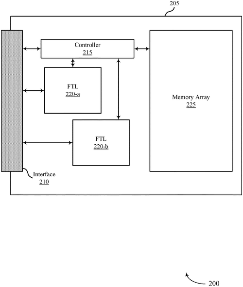
In a recent patent by Micron Technology, Inc., the company explores the concept of multiple flash translation layers (FTLs) within a memory device. This exciting development could potentially revolutionize the way data mapping is handled in memory devices. The patent describes a system where a memory device can support two or more FTLs, each with its own unique characteristics. One FTL might be configured to handle data mapping with a larger granularity, while another FTL could handle data mapping with a smaller granularity or data that doesn't match the defined granularity. The selection of which FTL to use is based on specific characteristics of the data being processed. The implications of this patent could be significant. With the ability to select the most appropriate FTL for handling different data characteristics, memory devices could potentially optimize data storage efficiency and performance. This could lead to faster and more efficient data transfers and improved overall user experience. While the concept described in the patent is intriguing, it is important to note that obtaining a patent does not guarantee that a product will be developed or brought to market. Therefore, it remains to be seen whether or not Micron Technology, Inc. will commercialize this innovative idea. In the current market, competitors such as Samsung and Western Digital dominate the memory device space. It will be interesting to see if they respond to this patent with their own developments or if they will continue to focus on their existing product lines. One can also imagine potential applications for this technology beyond memory devices. Could the concept of multiple FTLs be applied to other areas of data storage, such as solid-state drives or cloud storage solutions? The possibilities are intriguing, and it will be exciting to see how this patent influences future technological advancements. What are your thoughts on this patent? Do you believe that multiple FTLs in memory devices could enhance data storage and transfer capabilities? Share your thoughts and opinions in the comments below.
This document describes methods, systems, and devices for multiple flash translation layers (FTLs) at a memory device. A first FTL may be configured to support data mapping using a defined granularity and a second FTL may be configured to support data mapping using a smaller granularity than the defined granularity or data that does not match the defined granularity, based on one or more characteristics of the data. A memory device may select between the FTLs to map data based on the one or more characteristics of the data and may write the data to the memory device. The memory device may store logical-to-physical mapping associated with the data, among other information, using the selected FTL.
US Patent 11836074
Micron Technology, Inc.
A System Keeps Track of Data Lengths, and Updates L2P Mapping When Necessary
What is this invention?
Implementing mapping data structures to minimize sequentially written data accesses
A memory device and a processor,
Were coupled to make an L2P mapper.
It wrote data sequentially,
Then updated the LTU accordingly,
So that no one would be any the wiser.
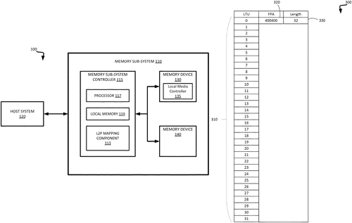
In a recently published patent, Micron Technology, Inc. introduces a system that aims to improve the efficiency of memory devices. The patent describes the integration of a memory device and a processing device, which work together to perform various operations. One notable feature of this system is the storage of logical-to-physical (L2P) mapping data on a volatile memory device. This data corresponds to sequentially written data, allowing for a more organized and streamlined approach to data management. The patent also outlines the system's ability to determine whether an L2P update criterion is met. Upon meeting this criterion, the system would then update an L2P mapping data structure based on the existing data. This mapping data structure is responsible for maintaining an initial logical translation unit (LTU) as well as tracking the length of the sequentially written data from the initial LTU. While this patent indicates an intriguing direction for the improvement of memory devices, it is important to note that obtaining a patent does not guarantee that a specific technology will be developed or brought to market. Competition within the tech industry is fierce, with existing products and solutions catering to many similar needs. However, if this system were to be developed, it could find potential applications in various industries. For instance, it could enhance the efficiency of data storage and retrieval in large-scale databases or help optimize data processing in complex computing systems. In sum, Micron Technology's patent presents an exciting concept that could potentially revolutionize memory devices. Whether or not this innovation will become a reality remains to be seen. What do you think about the idea proposed in this patent? Are there any potential uses you can envision for this technology? Let us know in the comments below!
The system includes a memory device, and a processing device, operatively coupled to the memory device. The processing device is configured to store, on the memory device, logical-to-physical (L2P) mapping data corresponding to sequentially written data. The processing device is also configured to determine whether an L2P update criterion is satisfied. In response to determining that the L2P update criterion is satisfied, the processing device updates an L2P mapping data structure based on the L2P mapping data. The L2P mapping data structure maintains an initial logical translation unit (LTU) of the sequentially written data, and a length of the sequentially written data from the initial LTU.
US Patent 11836076
Micron Technology, Inc.
Memory System Dynamically Tuning Host Performance Boost Thresholds
What is this invention?
Dynamically tuning host performance booster thresholds
A memory system for sure,
Dynamically tunes host performance too.
It may activate regions based on read commands,
And determine thresholds with ease and command.
For a dynamic boost of power to you!
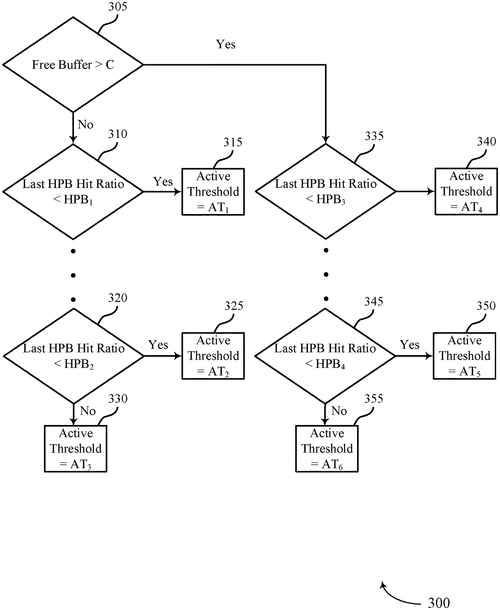
In a recent patent filed by Micron Technology, Inc., they have described methods, systems, and devices for dynamically tuning host performance booster thresholds. As per the patent, a potential memory system may include a set of memory devices and an interface that can communicate commands with a host system connected to the memory system. What makes this patent interesting is that the interface can communicate commands in two different modes. The first mode is associated with a logical address space, which consists of multiple regions. The second mode is associated with physical memory address. The controller within the memory system is responsible for determining the region activated for the second command mode and receiving the commands accordingly. Upon deactivating the region, the controller determines a threshold based on the quantity of read commands serviced in that mode. While the patent demonstrates a unique approach to dynamically tuning host performance booster thresholds, it is essential to remember that not all patents are successfully transformed into actual products. The tech industry is rife with innovative ideas that never make it to market due to various reasons such as feasibility, cost, or competition. It's interesting to speculate about the potential applications of this patent. If developed into a product, it could bring significant improvements to memory systems and enhance overall performance. However, it remains to be seen whether Micron Technology, Inc. will take this patent forward and turn it into a practical solution. What are your thoughts on this patent? Do you believe this innovation has the potential to disrupt the memory system market? Share your opinions in the comments below!
This document describes methods, systems, and devices for dynamically tuning host performance booster thresholds. A memory system may include a set of memory devices and an interface configured to communicate commands with a host system coupled with the memory system. The interface may communicate commands to the memory system according to a first command mode associated with a logical address space including a plurality of regions and communicate commands according to a second command mode associated with physical memory address. The controller may determine a region activated for the second command mode, receive a first plurality of commands, determine, upon deactivating the region, a first threshold based on a first quantity of read commands serviced according to the second command mode. The controller may activate the region for the second command based on a second quantity of read commands received exceeding the first threshold.
US Patent 11836077
Micron Technology, Inc.
Trim Settings on Memory Device Determined Based on Operational Characteristics
What is this invention?
Trim setting determination on a memory device
A device of memory needs trimming
So its operational state's glimmering
Determine the settings,
To ensure proper bettings,
For best performance without dimming.
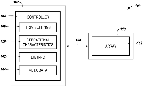
In a recent patent filing, Micron Technology, Inc. has introduced a potentially groundbreaking technology aimed at determining trim settings on memory devices. While this development may not grab headlines like the latest smartphone or virtual reality device, it holds substantial implications for the future of memory technology. The patent describes an apparatus that can determine a set of trim settings for the memory cells within the device. These settings are based on the operational characteristics of the memory array and are designed to achieve desired operational performance. Although the details are technical, the potential applications are vast. One could imagine this technology being employed in a variety of memory-intensive devices, such as smartphones, laptops, or servers. By optimizing the trim settings, memory devices could potentially offer enhanced speed, energy efficiency, and reliability. Competition in the memory market is fierce, with companies like Samsung and SK Hynix vying for dominance. Any new development that offers a competitive edge in terms of performance, energy efficiency, or cost-effectiveness could have a significant impact on the industry. However, it is important to note that a patent filing does not guarantee that a product will reach the market. Many patents end up sitting on shelves, never seeing the light of day. Therefore, it remains to be seen whether Micron Technology, Inc. will turn this innovative concept into a viable product. Looking ahead, it will be interesting to see if this patent leads to tangible advancements in memory technology. Will Micron Technology, Inc. be able to translate this concept into a commercial product that can disrupt the memory market? Or will this invention simply become another footnote in the history of technological innovations? What are your thoughts on this patent? Do you believe it has the potential to revolutionize memory devices, or do you remain skeptical about its practicality? Share your insights and opinions in the comments below!
The present disclosure includes apparatuses and methods related to determining trim settings for a memory device. The apparatus can determine a set of trim settings for the array of memory cells based on the operational characteristics of the array of memory cells, wherein the set of trim settings are associated with desired operational characteristics for the array of memory cells.
US Patent 11836078
SAMSUNG ELECTRONICS CO., LTD.
A Diagnosis Control Method of an Air Conditioner Is Provided to Clearly Inform a User of an Air Conditioner Installation Error
What is this invention?
Diagnosis control method of air conditioner
A diagnosis control method was found
For air conditioners all around.
It checks the state, and pipes too,
To tell you what's wrong with your view.
So no more installation errors abound!
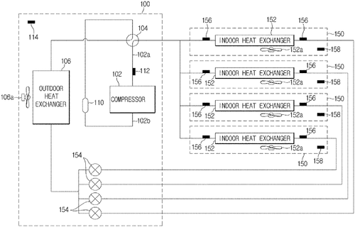
In a patent filed by Samsung Electronics Co., Ltd., a new diagnosis control method for air conditioners aims to provide clarity to users when it comes to installation errors. The method involves various steps, such as performing test runs to diagnose the assembly state, pipe connection, and refrigerant levels of the air conditioner. Based on the results of these tests, a determination is made, and the diagnosis result is displayed through a display device on the indoor unit of the air conditioner. On the surface, this concept seems like a practical solution to a common problem faced by both users and technicians. Air conditioner installation errors can be frustrating and time-consuming to identify, but this new method aims to simplify the process by offering clear diagnostics. Competitors in the air conditioning market, such as LG and Panasonic, already offer self-diagnosis features in some of their models. However, Samsung's patent appears to take it a step further by conducting multiple tests to thoroughly assess the air conditioner's state. If implemented successfully, this technology could have various applications. For instance, it could be used by homeowners as a quick and convenient tool during installation or maintenance. Additionally, HVAC technicians may find it beneficial in quickly identifying and resolving issues in a professional setting. However, as with many patents, the question remains whether this invention will make its way into actual products. While it showcases the potential for improved user experience and troubleshooting in the air conditioning industry, it's important to remember that not all patented technologies reach the market. What are your thoughts on this new diagnosis control method for air conditioners? Do you believe it could be a game-changer or simply an incremental improvement? Share your opinions and insights in the comments below.
The diagnosis control method includes receiving a test run command or a self-diagnosis command for diagnosis of the air conditioner, performing a first test run to diagnose an assembly state of the air conditioner, performing a second test run to diagnose pipe connection of the air conditioner and an amount of refrigerant in the air conditioner, performing a determination including diagnosing a state of the air conditioner based on operation results of the first test run and the second test run, and displaying the diagnosis result through a display device provided at an indoor unit of the air conditioner. The diagnosis control method is useful for informing users about installation errors with their air conditioning units.
US Patent 11835428
SAMSUNG ELECTRONICS CO., LTD.
New Optical Modulator Allows for Precise Control of Phase
What is this invention?
Fabry-Perot cavity phase modulator including a tunable core, an optical modulating device including the same, and a lidar apparatus including the optical modulating device
A tunable core of semiconductor,
To modulate a phase with much vigor,
It controls the light wave's course,
And allows for great force,
For precise manipulation of this figure.
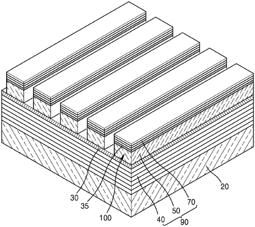
Samsung Electronics recently filed a patent for an innovative optical modulating device and the accompanying system. This device features a phase modulator, which is constructed on a substrate and incorporates a Fabry-Perot cavity. Within this cavity, there is a tunable core made of a semiconductor material that can effectively modify the phase of light. This modulation is achieved by controlling the refractive index of the tunable core through electrical means. The potential applications for such a device are vast, with possible implications in fields such as telecommunications, display technology, and photonics. By enabling precise control over the phase of light, this device could potentially enhance data transmission speeds, improve image quality in displays, or even contribute to the development of new technologies that rely on light manipulation. Of course, it's important to note that a patent filing does not guarantee that this device will become a mainstream consumer product anytime soon. Many factors come into play, such as technological feasibility, manufacturing challenges, and market demand. Additionally, it is crucial to consider the competitive landscape, with other companies already offering similar technologies or working on comparable solutions. For example, companies like Intel and IBM have made significant advancements in the field of optical modulators, with their own patented technologies. It remains to be seen how Samsung's approach compares to these competitors and whether it brings any unique advantages or improvements. In conclusion, Samsung Electronics' patent for an optical modulating device and its potential system is certainly an exciting development in the world of light manipulation. However, as with any patent, it's essential to take into account various factors before determining if and when this invention will translate into a viable product. What other applications do you think could benefit from precise control over the phase of light? Share your thoughts in the comments below.
The optical modulating device includes a substrate, and a phase modulator formed on the substrate and including a Fabry-Perot cavity. The Fabry-Perot cavity of the phase modulator includes a first reflective layer, a second reflective layer, and a tunable core formed between the first reflective layer and the second reflective layer, wherein the tunable core is formed of semiconductor material and is configured to modulate a phase of light corresponding to modulation of a refractive index of the tunable core according to electrical control. This allows for precise manipulation of light waves in order to create various effects.
US Patent 11835626
SAMSUNG ELECTRONICS CO., LTD.
Display apparatus and light source apparatus with improved reflectivity
What is this invention?
Display apparatus and light source apparatus thereof
A display apparatus had a light source,
Its protective layer was of course the force,
The first protection layer close to the diode,
And a second with less reflectance it showed.
This technology's quite hard to ignore!
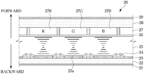
Samsung Electronics has recently filed a patent for a display apparatus and a light source apparatus, according to information disclosed. This invention includes a reflective sheet with a through hole, a light source placed in the through hole which contains a light emitting diode (LED), and a substrate to which the LED is attached. The substrate features a protection layer on one side, facing the reflective sheet. This layer consists of a first protection layer adjacent to the LED and a second protection layer with a lower reflectance than the first. While the technical details can be a mouthful, this patent offers promising potential applications. With the growing demand for brighter and more energy-efficient displays, Samsung's display apparatus might prove to be a game-changer. By utilizing the light emitting diodes and the reflective sheet, this invention could pave the way for displays that are not only visually stunning but also consume less power. One can't help but compare this development to the current market leaders in display technology. Competitors like LG and Apple have already been exploring similar innovations, such as OLED displays and MicroLED technology. However, Samsung's patent seems to take a different approach, focusing on the protection layer's distinct properties. How this unique feature will fare against existing solutions remains to be seen. Aside from improving display technology, there may be other potential applications for this invention. For instance, the use of light emitting diodes in a reflective sheet could have implications in architectural design, signage, or even automotive lighting. It will be interesting to see if Samsung, known for its versatility and vast product range, will leverage this patent to explore such applications. As with any patent filing, there is no guarantee that this concept will be developed into an actual product or make its way to consumer markets. However, the potential benefits of energy-efficient and visually impressive displays are undeniable. Would you be interested in purchasing a device featuring this technology? Let us know in the comments below!
The disclosure provides a display apparatus and a light source apparatus thereof. The light source apparatus includes a reflective sheet in which a through hole is formed, a light source disposed in the through hole and including a light emitting diode, and a substrate to which the light emitting diode is attached and including a protection layer disposed on one side facing the reflective sheet. The protection layer includes a first protection layer disposed adjacent to the light emitting diode, and a second protection layer having lower reflectance than the first protection layer.
US Patent 11835818
SAMSUNG ELECTRONICS CO., LTD.
New Reticle Reflects Extreme Ultraviolet Light for Precision Work
What is this invention?
Reticle in an apparatus for extreme ultraviolet exposure
A reticle with a multi-layer stack,
For the EUV light it would attract.
The absorber structure complete,
Capping layer so neat,
It'll make your exposure quite exact!
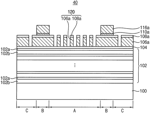
In a recent patent filed by Samsung Electronics, a new reticle for extreme ultraviolet (EUV) exposure is described. This innovative invention aims to improve the efficiency and performance of EUV exposure apparatuses used in manufacturing processes. The reticle consists of several key components. Firstly, it includes a substrate with an image area and a black border area surrounding it. On top of this substrate, a multi-layer structure is applied to reflect EUV light. A capping layer is then added to cover the multi-layer structure. Additionally, there are absorber layer patterns present on the capping layer in both the image area and the black border area. One interesting aspect of this patent is the absorber structure on the capping layer in the black border area. This structure is composed of sequentially stacked layers, including the first absorber layer pattern, a hard mask pattern, and a second absorber layer pattern. The absorber structure covers the entire upper surface of the capping layer in the black border area, providing increased functionality and precision. While this patent showcases Samsung's commitment to pushing the boundaries of technology, it is important to note that not all patented ideas make it to the production stage. The field of EUV exposure and semiconductor manufacturing is highly competitive, with companies like ASML dominating the market. It remains to be seen whether Samsung will successfully bring this invention to fruition and how it will compare to existing competitors' products. Looking ahead, the potential uses for this reticle patent are promising. Improved efficiency and performance in EUV exposure apparatuses could have far-reaching effects, impacting various industries reliant on semiconductor manufacturing, such as telecommunications, automotive, and consumer electronics. As readers, what are your thoughts on this patent? Do you believe Samsung will be able to commercialize this invention and compete with existing players in the market? Share your insights and opinions in the comments below.
The reticle in the apparatus for extreme ultraviolet (EUV) exposure includes a substrate with an image area and a black border area surrounding the image area. A multi-layer structure is on the image area and the black border area of the substrate, reflecting EUV light. A capping layer covers the multi-layer structure. First absorber layer patterns are on the capping layer in the image area and the black border area. An absorber structure is on the capping layer in the black border area, including one of first absorber layer patterns, a hard mask pattern, and a second absorber layer pattern sequentially stacked. The absorber structure covers an entire upper surface of the capping layer in the black border area.
US Patent 11835850
SAMSUNG ELECTRONICS CO., LTD.
New Photosensitive Composition Includes Quantum Dot Dispersions and Photopolymerizable Monomer with Carbon-Carbon Double Bond
What is this invention?
Photosensitive compositions, preparation methods thereof, quantum dot polymer composite prepared therefrom
A photosensitive composition was found
That included a quantum dot dispersion around
The acid group-containing polymer, so neat
Had two monomers with double bonds to meet
And the hydrophobic group was quite sound.

In a recent patent application, Samsung Electronics Co., Ltd. has introduced a photosensitive composition that includes a quantum dot dispersion, a photopolymerizable monomer with a carbon-carbon double bond, and a photoinitiator. The fascinating aspect of this invention lies in the quantum dot dispersion, which consists of an acid group-containing polymer and multiple quantum dots dispersed within it. The acid group-containing polymer is a copolymer comprising a first monomer with a carboxylic acid or a phosphonic acid group, along with a carbon-carbon double bond, and a second monomer with a hydrophobic group and without a carboxylic acid or phosphonic acid group. While the patent description seems complex and highly technical, it is important to note that filing a patent does not ensure that the invention will become an actual product. Samsung has a history of filing numerous patents, many of which may not see the light of day in the form of commercially available products. Therefore, it is crucial to approach this invention cautiously, acknowledging that it may merely be an exploration of possibilities rather than an indication of an upcoming consumer product. That being said, if commercialized, this photosensitive composition could have several potential applications. Quantum dots, which are semiconducting nanoparticles, have demonstrated their usefulness in various fields such as display technology and medical imaging. By integrating them into a photosensitive composition, novel applications in printing, imaging, and perhaps even advanced 3D printing could emerge. Imagine being able to capture precise images and recreate them with remarkable detail using a photopolymerizable monomer. Such technological advancements could revolutionize industries like photography, graphic design, and even manufacturing. However, it is important to remember that Samsung is not the only player in this field. Competitors like LG, Sony, and Panasonic have their own ongoing research and development processes, and it will be interesting to see if they come up with similar or more advanced products in the near future. As consumers, we can only hope that these pioneering inventions make their way to market, transforming the way we interact with technology. Now, dear readers, do you think this photosensitive composition utilizing quantum dots has the potential to disrupt existing industries? Are there any specific applications you can envision? Share your thoughts and insights in the comments below!
The text describes a photosensitive composition that includes a quantum dot dispersion and a photopolymerizable monomer. The quantum dot dispersion includes an acid group-containing polymer and a plurality of quantum dots dispersed in the acid group-containing polymer. The acid group-containing polymer includes a copolymer of a monomer combination including a first monomer having a carboxylic acid group or phosphonic acid group and carbon-carbon double bond and second monomer having carbon-carbon double bond and hydrophobic group, but not having carboxylic acid groups or phosphonic acid groups.
US Patent 11835856