Most innovative companies for 11/07/2023 (new inventions)
Exciting new inventions from International Business Machines Corporation, Micron Technology, Inc., Microsoft Technology Licensing, Llc, Dell Products L. P. And Intel Corporation
This is a weekly article summarizing a handful of inventions from the most innovative companies in the world. The summaries are created by an A. I. and proof-read by a human before publication. Attempts are made to ensure accuracy of the descriptions, but it is very much a work in progress. Each invention description is preceeded by a poem about the invention that is written by the A. I. I have found the limerick is actually quite good at explaining the invention in simple terms. Enjoy!
****
New Method of Illumination Creates Stunning Images in Turbid Media
What is this invention?
Method of inner light layer illumination by multi-beam interference and apparatuses for imaging in turbid media
A method of inner light layer illumation,
For optical imaging and detection in turbid formation,
The multiple beam interference creates a path to reduce absorption and scattering too,
Constructive interference forms an inner light layer for all that we view.
The theoretical analyses have been proven true,
And the designed apparatuses perform so well they'll blow you! The depth can reach five cm in human bodies or more than 500 m in clear seawater too, And resolutions <1 μm along object planes with 1 μm along direction of depth of field will do.
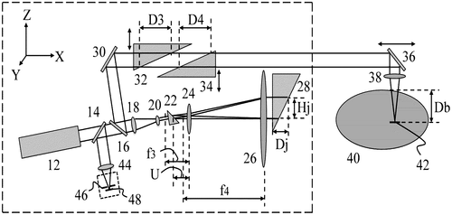
In a recent patent application, a new method of inner light layer illumination for optical imaging and detection in turbid media has been described. The invention claims to use multiple beam interference to manipulate the propagation path of light, thereby reducing absorption and scattering in turbid media. This method is said to enhance the signal strength by an impressive 600 dB compared to traditional technology. According to the theoretical analyses and mathematical calculations backing this invention, the designed apparatuses are expected to deliver outstanding performance. The imaging depth achievable with this method seems promising, with potential depths of over 5 cm inside the human body and more than 500 m in clear seawater. The imaging resolutions are touted as being less than 1 μm along the object plane and approximately 1 μm along the depth of field. While the potential applications of this technology are extensive, including medical imaging and underwater exploration, it's important to remember that obtaining a patent does not guarantee a product will come to market. Many factors, such as manufacturing feasibility, cost-effectiveness, and industry demand, need to be considered before such an invention turns into a consumer product. In the realm of medical imaging, there are already established players with their own devices and technologies. Will this new method be able to compete with existing imaging techniques, like MRI or CT scans, which have been refined over decades? And for underwater exploration, will the potential benefits outweigh the challenges of implementing this method in practical scenarios? What do you think? Could this new method of inner light layer illumination revolutionize optical imaging and detection? Share your thoughts in the comments below.
The invention relates to a method of inner light layer illumination for optical imaging and detection in turbid media. The method uses multiple beam interference to create destructive interference in the propagation path to reduce the illumination beam intensity, and so to reduce absorption and scattering of the turbid media. This creates constructive interference to produce composite light intensity maximum which forms an inner light layer to illuminate the object. The theoretical analyses and mathematical calculations have proved the feasibility of this method. The designed apparatuses have great performances, compared with the traditional technology. The imaging depth can be over 5 cm in human body, and more than 500 m in clear seawater. The imaging resolutions are <1 μm along object plane, and approximate 1 μm along direction of depth of field.
US Patent 11808568
****
Ocean Data Acquisition System Mounted to Existing Floating Body
What is this invention?
Sensor and telemetry unit (STU) adapted for securable coupling to a floating object or buoyant aid to navigation (AtoN) to operate as a selectively deployable ocean data acquisition system (ODAS)
A self-contained ocean data module,
Mounted to a floating body did roam.
It generated transfer functions based on motion characterization,
And used an existing body for its ocean acquisition.
To measure waves and other phenomena with precision!
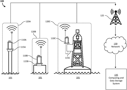
Apparatus and associated methods have been proposed for a self-contained ocean data and acquisition module (SCODAM). This innovative device is designed to mount onto a floating body and comes equipped with a sensor array, geospatial locating engine, wave measurement engine, communication engine, energy conversion module, and energy storage module. The SCODAM not only collects data but also converts ambient energy inputs into electrical energy, providing it with self-sustainability. One of the key advantages of this invention is its ability to repurpose existing floating bodies as ocean data acquisition systems (ODAS). This means that corporations or organizations could potentially gather valuable oceanographic data without the need for additional infrastructure or expensive new equipment. When imagining the potential uses for the SCODAM, it becomes apparent that it could greatly benefit industries such as marine research, environmental monitoring, and offshore energy production. By mounting SCODAM on buoys or platforms, scientists and engineers could gain valuable insights into wave motion and weather patterns, leading to more accurate predictions and informed decision-making for various applications. While the patent is certainly promising, it remains to be seen whether this invention will become a practical product. Competitor products already exist in the market, offering similar functionalities but often with different trade-offs. The challenge lies in making the SCODAM commercially viable, ensuring it meets the required performance standards and is cost-effective for widespread adoption. Nevertheless, this patent highlights the ongoing advancements in technology and their potential to revolutionize data collection in our oceans. How do you think the SCODAM would impact oceanic research and other related fields? Share your thoughts in the comments below.
This document describes a self-contained ocean data and acquisition module (SCODAM) that can be mounted to a floating body and used to collect data about waves, motion, and other ocean phenomena. The SCODAM is adapted to generate transfer function data based on motion characterization data obtained in a training mode, which can then be used to determine wave motion. This allows an existing floating body to be used as an ocean data acquisition system (ODAS).
US Patent 11808570
****
A Vibration Rectification Error Correction Circuit That Corrects Errors Quickly
What is this invention?
Vibration rectification error correction circuit, physical quantity sensor module, structure monitoring device, and correction value adjustment method of vibration rectification error correction circuit
A circuit for rectification error,
To improve accuracy and make it much clearer;
It uses biasing to get the right values,
And corrects errors with functions so able;
This circuit can help us measure physical quants - no terror!
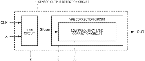
In a recent patent filing, a company has proposed a vibration rectification error correction circuit that aims to enhance the accuracy of sensor measurements. The circuit includes a first correction circuit, which utilizes a sensor element to measure a physical quantity and then corrects any vibration rectification errors present in the digital value obtained from the measurement. While the technical aspects of this patent may be intriguing, it remains unclear how this invention will be translated into a marketable product. Additionally, it's worth noting that some competitor products already offer similar functionalities in the realm of sensor accuracy improvement. Despite these challenges, one can imagine potential uses for this technology. For instance, in the field of motion sensors, where precise measurements are crucial, this vibration rectification error correction circuit could lead to more reliable data for applications such as virtual reality gaming or motion tracking in sports analytics. However, the success of this invention still depends on its practical implementation. Patents are often filed for ideas that never come to fruition, and it remains to be seen if this circuit will be commercialized or integrated into existing sensor technologies. In light of this patent, what other areas of technology and industry do you think could benefit from improved sensor accuracy? Let us know your thoughts and ideas in the comments below.
This text describes a vibration rectification error correction circuit, which corrects vibration rectification errors in digital values by using a correction function based on products of values obtained by biasing the digital value. This circuit can be used to improve accuracy and reliability of measurements made with sensor elements that detect physical quantities.
US Patent 11808572
****
Haptically-Enabled Directions for Sight and Hearing unimpeded
What is this invention?
System and method for providing directions haptically
A device that gives directions haptically
So you can both see and hear tactically
It has multiple units with output so neat
That it helps users find their way on the street
No need to look at your phone, no more audio instructions - sweet!
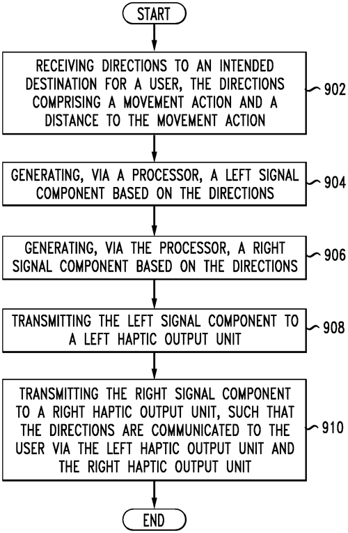
In a recently published patent, a new technology promises to revolutionize the way we receive directions while on the move. The patent describes systems, methods, and computer-readable storage devices that enable haptic feedback for providing directions, allowing sight and hearing to continue unimpeded. The patent envisions a wearable device, which could take the form of earphones, ear rings, gloves, glasses, or any other wearable object. This device receives directions to a user's intended destination, which include a movement action and the distance to that action. Utilizing multiple haptic output units, the wearable device generates a haptic output based on the directions received. This means users can receive directions through touch, eliminating the need to constantly refer to their mobile devices or rely on audio cues. Imagine walking down a crowded street with this wearable device discreetly guiding you through vibrations. No more staring at your phone or getting lost in audio directions, you can simply feel the vibrations that tell you when and where to turn, allowing you to keep your sight and hearing fully engaged with your surroundings. While this patent offers an intriguing solution to the problem of navigating while on the move, it is important to note that not all patented inventions make it to the market. The process of turning a patent into an actual product involves many challenges and considerations, including technological feasibility, market demand, and potential competition. Speaking of competition, some wearable devices, like smartwatches and fitness trackers, already offer limited haptic feedback for notifications and alerts. However, this new technology takes it a step further by applying haptic feedback to the realm of navigation. It remains to be seen how this patented invention will fare against potential competitors in the wearables market. So, dear readers, what are your thoughts on this innovative patent? Can you imagine any other valuable applications for haptic directions? Let us know in the comments below.
This invention provides a way for people to receive directions haptically, so that they can continue to see and hear what is happening around them. The wearable device has multiple haptic output units, which generate different types of haptic feedback based on the direction information. This allows users to receive the directions without having to look at their mobile devices or listen to audio instructions.
US Patent 11808598
****
A Measurement Circuit That Provides Precise Weight Information
What is this invention?
Measurement circuit for a body weight measuring apparatus for measuring body weight distribution
A Wheatstone bridge circuit was the key,
To measure body weight most accurately.
The amplifying and converting done right,
For a server to compute exact weight outright.
This load sensing unit powered by an input excitation voltage bright!
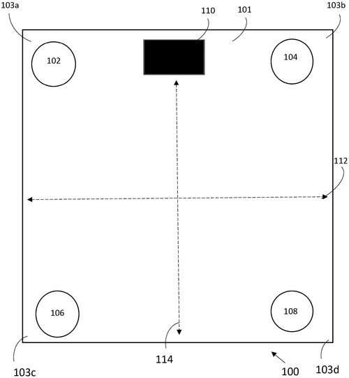
In the ever-evolving world of health and fitness technologies, a recently published patent describes a measurement circuit for a body weight measuring apparatus. This innovation is designed to revolutionize the way individuals track and monitor their weight, providing a more accurate and comprehensive analysis. While the patent showcases an impressive array of features, the question remains: will this invention actually make its way into the hands of consumers? At the core of this patent is a load sensing unit, which employs multiple wheatstone bridge circuits to generate weight information. By applying a load, the circuits produce an output voltage that represents various weight measurements, including left-side weight, right-side weight, anterior-side weight, and posterior-side weight. To power the load sensing unit, an input excitation voltage is applied across the wheatstone bridge circuits. The measurement circuit doesn't stop there. It also incorporates an amplifier circuit that magnifies the output voltage, generating an amplified output. This amplified output is then fed into an analog to digital converter circuit, which converts it into a digital representation of the load's weight. Finally, a microcontroller takes the digital weight representation and transmits it to a server, where an exact weight calculation can be performed. While this patent promises a more precise and data-driven approach to weight measurement, it is important to remember that obtaining a patent is just the first step in bringing an invention to market. Many factors come into play, including production costs, manufacturing feasibility, and market demand. Additionally, competitors already offer a range of body weight measuring devices, such as smart scales and fitness trackers, which add an additional layer of complexity for this patent's chances of becoming a consumer product. Despite these challenges, the potential uses for this technology are intriguing. Imagine a future where individuals can monitor weight distribution and make adjustments to their exercise or posture routines accordingly. Moreover, the ability to transmit weight data to a server could enable personalized feedback and recommendations from health professionals or fitness coaches. As we eagerly await the fate of this patent, it's worth contemplating its impact. Would you be interested in a body weight measuring apparatus that provides detailed weight distribution analysis? How could this invention enhance your health and fitness journey? Share your thoughts and opinions in the comments section below.
The text describes a measurement circuit for body weight. The load sensing unit includes at least one wheatstone bridge circuit that generates a load information comprising at least one of: left-side weight, right-side weight, anterior-side weight, and posterior-side weight in the form of an output voltage. The load sensing unit is powered by an input excitation voltage across the at least one wheatstone bridge circuit. The measurement circuit includes an amplifier circuit to amplify the output voltage to generate an amplified output, an analog to digital converter circuit for converting the amplified output to a digital representation of the weight of the load, and a microcontroller to receive and transmit the digital representation of the weight of the load to a server for computing an exact weight of the load.
US Patent 11808617
International Business Machines Corporation
Wafer Probe Adapter Plate for Accommodating Single Chip Easily Found
What is this invention?
Testing a single chip in a wafer probing system
A wafer probing system with a chip,
Must be tested to give it the whip.
An adapter plate loaded up tight,
To determine its exact position in search light.
Then test routines are stored for a dip,
In the controller of the wafer probing system so quick!
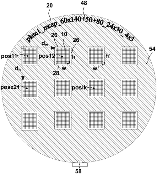
In a recently published patent, International Business Machines Corporation (IBM) has unveiled a method for testing single chips within a wafer probing system. The patent describes the use of an adapter plate with an interface surface, designed to accommodate the single chip, which is then loaded into the wafer probing system. Once loaded, the system determines the precise position of the chip in the adapter plate and proceeds to test it using pre-defined test routines stored in the system's controller. On the surface, this method seems like a logical approach to efficiently test individual chips in a wafer probing system. However, it is important to note that a patent does not guarantee that a product will be developed or released. While IBM is a leader in the technology industry, there is no information at this time regarding their plans to bring this particular invention to market. Competitors in the wafer probing system space, such as Teradyne and FormFa. ctor, already offer various solutions for testing chips in a wafer-scale environment. These companies have established product lines and customer bases, making it challenging for new entrants to disrupt the market. It remains to be seen if IBM's patent will result in a compelling product that can compete with existing offerings. That being said, the potential use cases for a method like IBM's are intriguing. More efficient testing processes can have a significant impact on chip production, ensuring higher quality components and reducing time and cost. If IBM can successfully develop and release a product based on this patent, it may find its place in the industry. As we eagerly await further news from IBM, we must ponder the following question: How significant are more efficient testing methods in improving chip production and overall technology development? Let us know your thoughts in the comments below.
The method for testing at least one single chip in a wafer probing system includes loading an adapter plate with the at least one single chip into the wafer probing system and determining an exact position of the at least one single chip in the adapter plate in the search area. The method then tests the at least one single chip with test routines stored in a controller of the wafer probing system.
US Patent 11808808
International Business Machines Corporation
An Easy Way to Detect Computer System Anomalies
What is this invention?
Root cause analysis of computerized system anomalies based on causal graphs
A root cause analysis for computerized systems was made
It monitored KPIs and detected an anomaly in the grade
The troubleshooting time window was then defined
Strict subsets of KPIs were identified
And the causal graph with paths returned
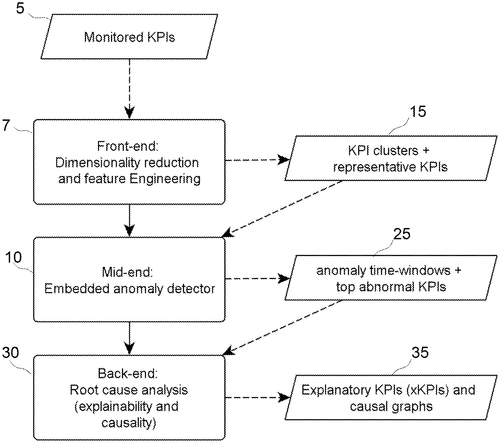
International Business Machines Corporation has recently filed a patent for an intriguing invention aimed at enhancing computerized system management. This embodiment offers a method for conducting root cause analysis of anomalies within computer systems, bringing a potential solution to the long-standing challenge of identifying and troubleshooting system issues. The patent outlines a multi-step process, starting with the monitoring of key performance indicators (KPIs) within a computerized system. These KPI values form respective time series, which are then analyzed to detect any anomalies. Upon identifying an anomaly, the system determines a troubleshooting time window, restricting the analysis to a specific period for more accurate results. Next, a strict subset of the monitored KPIs is identified, which includes abnormal KPIs (aKPIs) and potential explanatory KPIs (xKPIs). By utilizing portions of the time series data spanning the troubleshooting time window, this subset assists in honing in on potential causes for the anomaly. The patent further describes the process of obtaining a causal graph, mapping the KPIs of the strict subset using a causality algorithm. This algorithm evaluates the weights of directed edges that connect the vertices, providing insight into potential causal relationships among the identified KPIs. Finally, the obtained causal graph is returned, offering a visual representation of the potential causes contributing to the system anomaly. While this patent showcases IBM's commitment to innovation and problem-solving within computer systems, it is important to note that filing a patent does not guarantee that the invention will become a reality. As with any patent, it will be interesting to see if IBM can successfully translate this concept into a practical product that can be implemented in real-world scenarios. The potential uses for this embodiment are considerable. For example, software development companies could benefit from easily identifying the root cause of system anomalies, allowing for faster resolutions and improved user experiences. Additionally, businesses relying on complex computer systems, such as financial institutions or large-scale manufacturing plants, could leverage this invention to minimize downtime and maximize productivity. Considering the numerous existing contenders in the computer system management space, such as Microsoft's System Center Operations Manager and SolarWi. nds Network Performance Monitor, it remains to be seen whether IBM's patent will bring forth a revolutionary product that can disrupt the market. Nevertheless, the concept described is undoubtedly thought-provoking and could potentially address a longstanding pain point in the industry. What do you think of IBM's patent for root cause analysis? Do you believe this invention has the potential to revolutionize computer system troubleshooting? Share your thoughts and predictions in the comments below.
An embodiment for root cause analysis of computerized system anomalies is provided. The embodiment may include monitoring key performance indicators (KPIs) for a computerized system, wherein KPI values of the monitored KPIs form respective timeseries. The embodiments may include detecting an anomaly in the computerized system based on the monitored KPIs. The embodiments may include determining a troubleshooting time window extending over a given time period. The embodiments may include identifying a strict subset of the monitored KPIs based on portions of the respective timeseries spanning the given time period. The subset comprises abnormal KPIs (aKPIs) and potential explanatory KPI (xKPIs). The embodiments may include obtaining a causal graph of vertices mapping KPISof the strict subset by running a causality algorithm to evaluate weights of directed edges connecting the vertices and accordingly obtain one or more directed paths. The embodiments may include returningthe obtained causal graph
US Patent 11809267
International Business Machines Corporation
Computer Processors Determine Storage Strategy for Chunked Data Blocks in Training Dataset
What is this invention?
Defining redundant array of independent disks level for machine learning training data
A computer system was devised
To store data blocks in RAID guise
The usefulness score, it did compute
For each block in the training route
Striping, mirroring and double parity to boot!
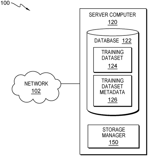
In a recent patent application, International Business Machines Corporation (IBM) has described a new technique for determining storage strategies for data blocks in a training dataset. By using computed usefulness scores and a series of usefulness thresholds, the method aims to optimize data storage by employing various RAID (Redundant Array of Independent Disks) strategies such as striping, mirroring, parity, and double parity. RAID, a technology widely used in storage systems, allows for a combination of data redundancy and improved performance. It achieves this by dividing data into blocks and distributing them across multiple disks. The benefits of this approach are clear, as it helps protect against data loss and ensures a system's smooth operation even in the event of disk failures. IBM's proposed strategy goes even further, using computed usefulness scores to determine the most effective storage approach for each data block. By considering the specific characteristics of the data and applying predefined thresholds, the system would optimize the storage allocation, ensuring that each block is placed in the most suitable RAID category. While the concept behind IBM's patent application is fascinating, it's important to remember that not all patented technologies see the light of day as practical products. Although IBM has a strong record of translating research into real-world solutions, the implementation and market viability of this specific technique remain to be seen. Some potential applications of IBM's storage strategy could be in industries dealing with large datasets, such as scientific research, finance, or even cloud computing. Being able to efficiently store and retrieve data is crucial in these fields, and any improvement in performance and reliability would be highly valued. Considering the current availability of competitors' RAID solutions, such as those offered by storage giants like Dell EMC and Hewlett Packard Enterprise (HPE), it will be interesting to see if IBM's method can provide a distinct advantage. Will this patented technique truly revolutionize the storage industry, or is it simply an inventive concept that may not materialize as a practical product? What do you think of IBM's proposed approach to data storage? Can you envision any specific scenarios where this technique could be a game-changer? Share your thoughts in the comments below.
This text describes a computer system that uses RAID strategies to store data blocks. The computer system determines a storage strategy for each chunked data block in a training dataset based on a respective computed usefulness score and a series of usefulness thresholds. The storage strategy comprises one or more RAID strategies, such as striping, mirroring, parity, and double parity. The computer system then distributes each data block in the training dataset according to the respective determined storage strategy.
US Patent 11809373
International Business Machines Corporation
Multi-dimensional data labeling: Consolidating dimension labels into one row label
What is this invention?
Multi-dimensional data labeling
A data set with attributes, so neat
It was split up into many a feat
The labels for each row
Were consolidated to show
How multi-dimensional it can be!
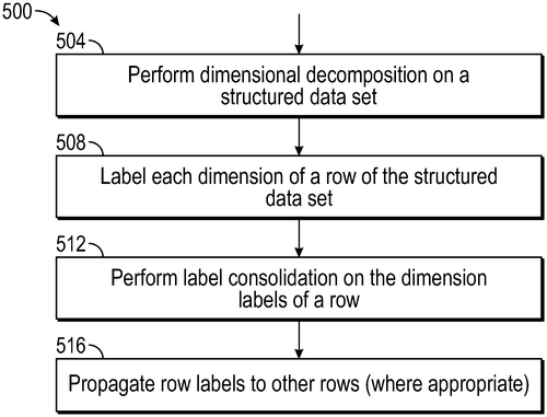
International Business Machines Corporation (IBM) has recently filed a patent for their innovative method and system called "Methods and Systems for Multi-Dimensional Data Labeling." This technology aims to revolutionize how structured data sets are organized and labeled. In simple terms, this system takes a structured data set with multiple rows and breaks it down into different dimensions, each representing a specific subset of data attributes. The decomposition is based on a coherence criterion, ensuring that each dimension is logically connected. Additionally, dimension labels are obtained for each dimension of selected rows, and these labels are then consolidated into row labels for easier identification and categorization. While the concept of multi-dimensional data labeling may seem complex, the potential applications of this technology are intriguing. For instance, imagine implementing this system in large-scale e-commerce platforms where millions of products and attributes require precise categorization. By efficiently organizing and labeling data, it could enhance search capabilities, improve recommendations, and streamline operations for businesses and customers alike. Competitors in this space, such as Amazon and Google, have also been investing heavily in data organization and categorization. However, IBM's approach seems distinct, with its emphasis on breaking down data into dimensions and utilizing coherence criteria. The patent application suggests that IBM is serious about this invention, but it remains to be seen whether it will translate into a tangible product. As with any patent, it is important to remember that not all filed innovations turn into commercially available products. Nevertheless, the idea of multi-dimensional data labeling undoubtedly holds promise. What potential uses do you envision for this technology beyond e-commerce? How do you believe it could impact other industries or sectors? Share your thoughts in the comments below!
This document describes methods and systems for multi-dimensional data labeling. A structured data set is obtained, the structured data set comprising a set of data attributes. Each data attribute has a data value for each of the plurality of rows of the structured data set. The structured data set is decomposed into a plurality of dimensions, each dimension defining a proper subset of the data attributes based on coherence criterion. A dimension label is obtained for each dimension of at least a portion of the plurality of rows of the structured data set and the dimension labels for a given one of the rows are consolidated into at least one row label for the given one of the rows.
US Patent 11809375
International Business Machines Corporation
A File System for Multiple Architectures That Is Responsive and Fast
What is this invention?
Building a file system for multiple architectures
A process for building a file system,
Retrieve layers from cache as you list'em,
Repeat until each layer's built,
Then store just one image of the result,
And your work is done - mission accomplished!
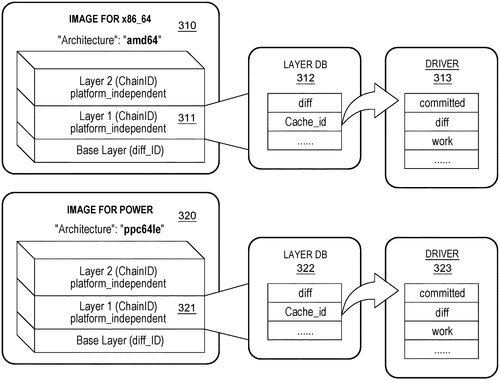
In a patent filed by International Business Machines Corporation (IBM), the company proposes a new approach to building a file system for multiple architectures. The concept revolves around a responsive process that retrieves and builds various layers, ultimately resulting in a single image of a complete file system that supports each platform. The patent outlines a systematic method wherein a base layer, which serves as an operating system base, is retrieved for each platform to be built. If any layer is yet to be built, the next layer is fetched. If the next layer is platform-independent, it is retrieved from a cache that supports all platforms. However, if the next layer is platform-dependent, a copy of the layer is built for each platform. This iterative process continues until each layer is built, and finally, a single image of the file system is stored, designed to work seamlessly across various architectures. While this proposal showcases the potential for efficient file system construction for multiple platforms, it is important to note that it is merely a patent at this stage. It remains to be seen whether IBM will bring this invention to life as a practical product. Moreover, competing products such as file systems designed specifically for individual architectures may pose challenges to its market feasibility. However, one can imagine the potential utility of such a system, especially in large organizations or across different operating systems. Streamlining file system builds across multiple platforms could bring about significant time and cost savings. As we await future developments, it would be interesting to hear from our readers: Do you think a unified file system build for multiple architectures would be a game-changer? How would it impact your work or organization? Share your thoughts in the comments below.
The text describes a process for building a file system, where layers are retrieved from a cache as needed. The process is repeated until each layer is built. Once the layers are built, a single image of the completed file system is stored.
US Patent 11809376
Micron Technology, Inc.
Thermal Chamber Keeps Electronics Cool and Protected
What is this invention?
Standalone thermal chamber for a temperature control component
A thermal chamber was designed to fit,
To mount a circuit board in it.
One side had ports for components galore,
For controlling the temperature and more.
The electronic system above could be seen,
Thanks to the clever patent machine!
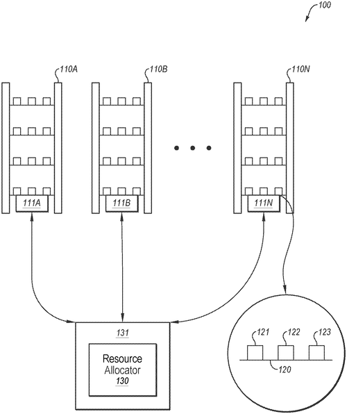
Micron Technology, Inc. has recently filed a patent for a thermal chamber with multiple sides that form an enclosed chamber. This innovative design aims to provide an adjustable mounting solution for electronic circuit boards, ensuring optimal thermal control for the components within. The key feature of this patent is the inclusion of one or more ports on the second side of the chamber. These ports enable the attachment of temperature control components, which can transfer thermal energy locally to and from a plurality of electronic devices in an electronic system positioned above the circuit board. While this patent showcases Micron's commitment to improving thermal management in electronic systems, it is important to note that it is not a product announcement. It is merely a filing that outlines a potential solution. As with many patents, there is no guarantee that this design will make it to market in the form described. Competition in the field of thermal management is fierce, with numerous companies offering solutions to address the growing need for effective cooling in electronic devices. Established players like Cooler Master, Noctua, and Corsair already offer an array of cooling solutions, ranging from fan-based to liquid cooling systems. If this invention were to become a reality, its applications could be vast. Electronic circuits generate heat, and efficient thermal management is crucial to ensure their longevity and prevent performance degradation. From consumer electronics to data centers, the need for effective cooling solutions remains constant. Considering the significance of thermal control in our technology-driven world, it becomes essential for companies to invest in innovative solutions to address this challenge. This patent from Micron promises a potential breakthrough in thermal management, but only time will tell if it becomes a reality. What are your thoughts on this technology? Do you believe Micron's thermal chamber design has the potential to revolutionize the way we cool electronic devices? Share your insights in the comments below.
The thermal chamber described in the patent includes a first side that is adjustable to mount an electronic circuit board within the chamber. The second side of the thermal chamber has one or more ports that expose the chamber, and each port is configured to receive a temperature control component. These components are used to transfer thermal energy locally to and from a plurality of electronic devices of an electronic system that is coupled to and positioned above the circuit board.
US Patent 11808803
Micron Technology, Inc.
Memory Test System Selects Unused Test Resources for Assigned Tests
What is this invention?
Allocation of test resources to perform a test of memory components
A system was crafted with great care,
To test memory components there.
It identified the resources of a platform,
And from those it chose a subset to form.
Finally assigning them for use in the test,
Giving accurate results at its best!
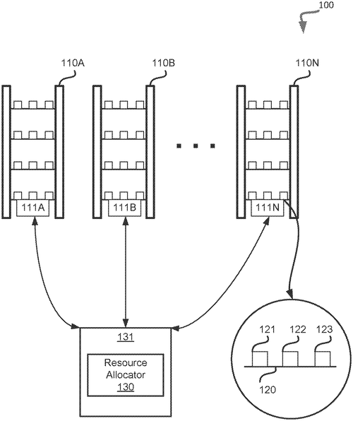
Micron Technology, Inc. has recently filed a patent for a system that aims to optimize the testing process of memory components. The invention, if successfully developed and implemented, has the potential to revolutionize the efficiency and speed at which memory components are tested within a test platform. The system, as described in the patent, comprises a memory component and a processing device. When a request is received to perform a first test of memory components, the processing device identifies the test resources associated with these components within the test platform. It then proceeds to find a subset of test resources that are not being utilized by a second test of the memory components. The innovation lies in the ability of the system to intelligently assign the unused test resources to obtain an assigned test resource for use in the initial test. By doing so, the system optimizes resource allocation, potentially reducing testing time and improving overall efficiency. While this invention appears to be a promising step forward in the realm of memory component testing, it is important to note that a patent filing does not guarantee the development of a commercial product. Patents are often filed to protect intellectual property, and it remains to be seen whether Micron Technology, Inc. will bring this specific invention to market. Competitors in this domain, such as Samsung and Intel, already offer a range of memory components and related testing solutions. It will be interesting to see if they can leverage similar technologies to further enhance the testing process or if this patent will give Micron Technology a unique advantage. This groundbreaking invention has the potential to streamline testing procedures, leading to faster and more efficient development of memory components. Beyond the realm of memory components, one can imagine the application of this technology in various industries that rely on testing and validation processes. What are your thoughts on this new patent by Micron Technology, Inc.? Do you believe it will make a substantial impact on the efficiency of memory component testing? Share your insights in the comments below.
A system includes a memory component and a processing device, operatively coupled with the memory component, to receive a request to perform a first test of memory components at a test platform. The system then identifies test resources of the test platform that are associated with the memory components. The system also identifies, among the test resources, a subset of test resources that are not being used by the second test of the memory components at the test platform. Finally, based on the subset of thetest resources, the system assigns one or more ofthetestresourcesto obtain an assignedtestresourcefor use bythetest.
US Patent 11808806
Micron Technology, Inc.
Host-Based Memory Device Maintenance Made Easy
What is this invention?
Host-based flash memory maintenance techniques
A host could manage a memory device,
It would receive write info which was encrypted.
The data to be written,
Would then have to be smitten,
For the memory device maintenance statistics updated and kept.

In a recent patent filed by Micron Technology, Inc., exciting advancements in flash memory maintenance have been revealed. The patent introduces a technique that allows host-based maintenance of a flash memory device, opening up new possibilities for improved performance and efficiency. One of the key features of this invention is the encryption of memory write information at the device level, providing the host with secure access to update and maintain memory device maintenance statistics. This approach could potentially enhance the overall reliability and longevity of flash memory devices, as it enables the host to closely monitor and optimize their performance. While the concept is undoubtedly intriguing, it remains to be seen whether this invention will evolve into a tangible product. As with any patent, numerous factors, such as market demand, technical feasibility, and competition, come into play. Micron Technology faces tough competition in the flash memory market, with established players constantly striving to innovate and improve their offerings. If ultimately developed into a product, this technology could find applications in various industries. For example, in the field of data centers, where flash memory plays a crucial role in handling vast amounts of data, host-based maintenance could lead to smoother operations and higher efficiency. Additionally, in sectors that rely heavily on flash memory, such as digital recording devices or high-performance computing, this innovation could significantly enhance overall system performance. As we anxiously await whether Micron Technology will bring this concept to fruition, what are your thoughts on the potential impact of host-based flash memory maintenance? Do you foresee any specific use cases or have any concerns about its implementation? Share your insights and thoughts in the comments below.
In certain examples, a memory device can be managed by a host. The host can receive write information for the memory device, which can be encrypted. The encrypted write information can include data that is to be written to the memory device. The data can be decrypted by the host and used to update and maintain memory device maintenance statistics.
US Patent 11809311
Micron Technology, Inc.
Storing Data with Tokens: Completion Indicator
What is this invention?
Tokens to indicate completion of data storage
A system of tokens, no doubt,
Will tell the host when data's stored out.
The open transaction token will start it off,
And then a safety token to scoff.
So that memory cells in an array can be stocked!
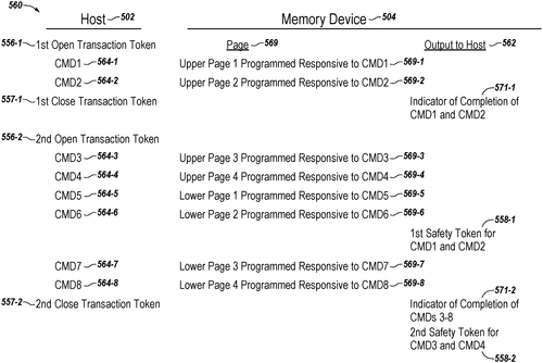
Micron Technology, Inc. has recently obtained a patent for a new system that aims to indicate completion of data storage to memory. The patent describes a method that involves storing data values in memory cells based on commands received from a host and using tokens to track the completion of the storage process. In simple terms, this technology allows for the organization of data storage by using tokens as indicators of completion. For instance, upon receiving a command from a host, the system stores a number of data values in a designated area of a memory array. Then, when the host sends a second command to store more data values in the same area, a safety token is transmitted back to the host to signify that the previous storage operation has reached completion. This patent indicates that Micron Technology, Inc. is exploring ways to optimize data storage processes by improving efficiency and tracking progress. While the concept itself seems promising, it is important to note that acquiring a patent does not necessarily mean that a product based on the patent will be created and brought to market. Patents are often obtained as a means of intellectual property protection, and companies may decide to explore or incorporate various ideas without necessarily finalizing them into consumer products. In terms of potential applications, this system could be beneficial in sectors where efficient data storage and management are crucial, such as cloud computing, database management, and artificial intelligence. By providing a clear indication of completion, it may help in reducing errors and improving overall system performance. It is interesting to consider how this technology would stack up against existing solutions in the market. Currently, competitors offer various methods for tracking the completion of data storage, such as checksums or flags. Are tokens a more effective and reliable approach? Are there any potential drawbacks or limitations to this token-based system that need to be addressed? Feel free to share your thoughts on this patent and its potential impact on data storage in the comments below.
This text describes systems, apparatuses, and methods related to tokens that indicate completion of data storage in memory. An example method may include storing a number of data values by a first page in a first row of an array of memory cells responsive to receipt of a first command from a host, where the first command is associated with an open transaction token. Additionally, the method may include sending a safety token to the host to indicate completion of storing the number of data values by the second page in the first row.
US Patent 11809324
Micron Technology, Inc.
Recovering L2P Table Info for Memory Devices in a Timely Manner
What is this invention?
Recovery of logical-to-physical table information for a memory device
A memory system needs to be able,
To recover L2P table information stable.
It can detect an error with a code uncorrectable,
Determine a set of candidate codewords collectible.
The logical address must match the metadata that's factual,
If no other candidates remain then it's successful!
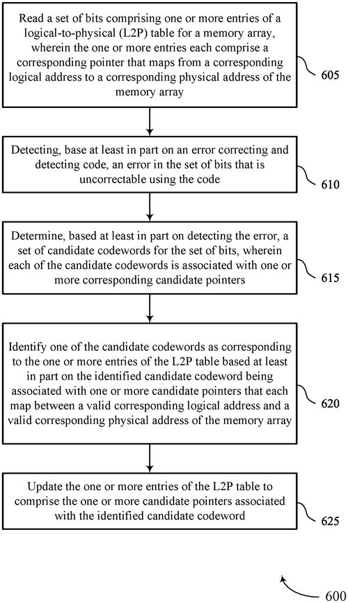
A recent patent from Micron Technology, Inc. unveils some intriguing methods, systems, and devices for recovering logical-to-physical (L2P) table information for memory devices. In simple terms, this technology aims to address errors in the L2P table using an uncorrectable error detecting code. By detecting these errors, the memory system can then determine a set of candidate codewords, each consisting of one or more corresponding candidate pointers. These candidate codewords are then checked to see if they are correct by comparing the logical address they point to with the metadata stored for a specific set of data at the physical address. The memory system can further streamline the process by limiting or ordering the candidate codewords, thereby reducing latency associated with identifying the correct codeword. While this patent certainly dives deep into the inner workings of memory systems, it remains to be seen how practical and commercially viable this technology will be. Memory systems are a crucial component of various devices, ranging from smartphones and laptops to servers and data centers. Competitors in the market, such as Samsung and Intel, continuously strive to improve memory performance and reliability. Therefore, any advancements in the recovery and error correction processes would undoubtedly attract attention. The potential uses for this technology are vast and could benefit a wide range of industries. In data centers, for example, where large amounts of data are stored and processed, the ability to quickly and accurately recover L2P table information could lead to improved system performance and reduced downtime. In consumer electronics, such as smartphones or tablets, this technology could enhance the stability and reliability of memory, preventing data corruption and loss. As promising as this patent may sound, it's worth considering the practical challenges and feasibility of implementing such a complex system. Will this technology prove to be a game-changer for memory devices, or will it remain confined to the realms of theoretical innovation? Only time will tell. What are your thoughts on this patent? Do you believe the recovery of L2P table information is a significant challenge in memory systems? Share your insights in the comments below.
This document describes methods, systems, and devices for recovering logical-to-physical (L2P) table information for a memory device. An error in one or more pointers of the L2P table may be detected using an error detecting code that is uncorrectable using the code. The memory system may determine a set of candidate codewords for the set of bits, where each of the candidate codewords includes one or more corresponding candidate pointers. The memory system may check whether a candidate codeword is correct based on whether a logical address corresponding to a candidate pointer of the candidate codeword matches a logical address stored as metadata for a set of data at a physical address pointed to by the candidate pointer. If the candidate codeword is not correct, then another candidate codeword may be evaluated. If no other candidates remain, then the correct Candidate Codeword has been identified and can be used to recover data from the L2P table.
US Patent 11809329
Microsoft Technology Licensing, LLC
A Method to Evaluate a Semiconductor-Superconductor Heterojunction for Use in a Qubit Register of a Topological Quantum Computer
What is this invention?
Pre-screening and tuning heterojunctions for topological quantum computer
A method was devised to measure
The admittance and conductance of a treasure
For use in qubit register,
Analysis of data made it better
And found the topological phase with pleasure
Microsoft Technology Licensing, LLC has recently filed a patent that outlines a method to evaluate a semiconductor-superconductor heterojunction for possible use in a qubit register of a topological quantum computer. The patent describes a process that involves measuring the radio-frequency (RF) junction admittance and the sub-RF conductance of the heterojunction to gather mapping data and refinement data. This information is then analyzed to identify regions in a parameter space that align with an unbroken topological phase of the heterojunction. Additionally, the refinement data helps find the boundary of the unbroken topological phase and the topological gap of the heterojunction within these regions. While this patent showcases Microsoft's commitment to advancing quantum computing technology, it is important to consider its practical implications. It is crucial to note that a patent filing does not necessarily guarantee that a product based on this invention will become a reality. Numerous factors come into play, such as technical feasibility, scalability, and market demand. Other companies in the quantum computing space, such as IBM and Google, have made significant progress in developing their own approaches to qubit registers and topological quantum computers. This patent by Microsoft could potentially be an important addition to the competition, but it remains to be seen if it will materialize into a tangible product. If successfully implemented, this technology could revolutionize the field of quantum computing by enabling more efficient and stable qubit registers. This, in turn, could lead to advancements in various fields like cryptography, drug discovery, and optimization problems. What are your thoughts on the potential of topological quantum computing? Do you believe it will become a reality and, if so, how do you foresee it impacting various industries? Share your insights in the comments below.
This method evaluates a semiconductor-superconductor heterojunction for use in a qubit register of a topological quantum computer. The method includes measuring one or both of an RF junction admittance and a sub-RF conductance, to obtain mapping data and refinement data. Then, by analysis of the mapping data, one or more regions of a parameter space consistent with an unbroken topological phase of the semiconductor-superconductor heterojunction are found. Finally, by analysis of the refinement data, a boundary of the unbroken topological phase in the parameter space and a topological gap of the semiconductor-superconductor heterojunction for at least one of the one or more regions of the parameter space are found.
US Patent 11808796
Microsoft Technology Licensing, LLC
Wearable Devices With Improved Hinge Electrical Connections
What is this invention?
Locating electrical contacts on device hinge
A wearable device was made in haste,
With a frame and two temple pieces in place.
Two hinges connected them well,
And contacts were there to tell,
External circuitry it could embrace!

In a recent patent application filed by Microsoft Technology Licensing, LLC, an intriguing new concept has emerged: a wearable device with electrical contacts arranged on its hinges. While the patent does not explicitly describe a specific product, it suggests the development of a novel wearable technology that could potentially change the game in the industry. The proposed device features a frame and two temple pieces connected to it via hinges. These hinges are equipped with electrical contacts, which are designed to connect with external circuitry. This innovative configuration opens up a world of possibilities for the wearable device. One possible application for this technology could be in the field of smart eyewear. Imagine a pair of augmented reality glasses with embedded sensors and miniaturized circuits, seamlessly integrated into the hinges. These electrical contacts could facilitate data transfer, power supply, or even communication with external devices, allowing for a more streamlined and efficient user experience. While it's exciting to envision the potential uses for such a device, it's important to remember that not all patented technologies make it to the consumer market. The innovation landscape is filled with numerous ideas that never see the light of day beyond the patent office. Moreover, this concept faces competition from already established wearable devices, such as smartwatches and fitness trackers. These products have already carved out a space in the market, with established brands and user bases. It remains to be seen whether Microsoft or other companies will take this patent and transform it into a commercially viable product that can compete with the likes of Apple, Fitbit, or Samsung. In the world of technology, patents are just the first step. It takes a combination of market demand, manufacturing capabilities, and consumer adoption for an idea to evolve into a tangible product. So, while the notion of wearable devices with electrical contacts on hinges is undeniably captivating, it ultimately falls upon the industry and consumers to determine its fate. What are your thoughts on this patent? Can you imagine any innovative uses for wearable devices with electrical contacts on their hinges? Share your insights and ideas in the comments below!
A wearable device is disclosed that includes a frame, first temple piece, second temple piece, first hinge connecting the first temple piece to the frame, second hinge connecting the second temple piece to the frame, and first contact and second contact arranged on one or more of the first hinge and the second hinge. The first contact and the second contact are configured to connect with external circuitry.
US Patent 11809020
Microsoft Technology Licensing, LLC
System Detects Type, Generates Customizable User Interface
What is this invention?
Rules based user interface generation
A system was made to build a UI,
It had a processor that would try.
To detect the type of the system with ease,
And execute a manager to please.
A layout of rules then it could supply!
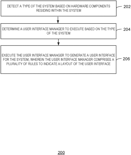
In a recent patent filing, Microsoft Technology Licensing, LLC has proposed a system that aims to revolutionize user interfaces. The patent describes a processor that can detect the hardware components of a system and generate a user interface accordingly. By determining the type of system and executing a user interface manager, the processor can generate a user interface layout based on a set of rules. If implemented, this technology has the potential to enhance user experiences across a range of devices. Imagine a smartphone that automatically adjusts its interface based on the specific hardware components it contains, or a smart home system that intuitively adapts its user interface to the connected devices. The possibilities are endless. While Microsoft's patent presents an intriguing concept, it is important to remember that not all patents lead to actual products. Many factors come into play during the development and commercialization process, including technical feasibility, market demand, and competition from other companies. It will be interesting to see if Microsoft turns this invention into a real-world product. Speaking of competition, companies like Apple and Google have long been at the forefront of user interface innovation. Apple's iOS and Google's Android operating systems have evolved significantly over the years, offering a seamless and intuitive user experience across various devices. It remains to be seen how Microsoft's proposed system will fare against these established competitors. As with any technological advancement, there are questions that arise. How well would this system adapt to different hardware configurations? Will users embrace the idea of a dynamically changing user interface? What potential challenges might arise during implementation? What do you think? Do you believe Microsoft's patent has the potential to revolutionize user interfaces? Share your thoughts and insights in the comments below.
This text describes a system that can generate a user interface. The system includes a processor to detect the type of the system, and determine a user interface manager to execute based on the type of the system. The processor can also execute the user interface manager to generate a user interface for the system. The type of the user interface manager can include a plurality of rules to indicate a layout of the user interface.
US Patent 11809217
Microsoft Technology Licensing, LLC
Interconnecting capacitive and inductive elements in a resonant capacitively-coupled rib
What is this invention?
Topologies for interconnecting capacitive and inductive elements in a capacitively-coupled rib
A RCN was designed for the task,
To interconnect capacitive and inductive mask.
The rib had a spine with two lines of cap',
One line got signal one, the other tap.
And an inductive line to join them direct,
For resonating in response to clock effect!
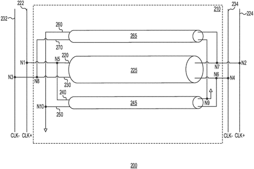
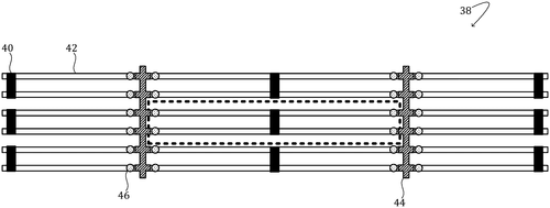
In the latest patent application by Microsoft Technology Licensing, LLC, a fascinating concept of interconnecting capacitive and inductive elements in a capacitively-coupled rib is unveiled. This groundbreaking innovation is directed towards the development of a resonant clock network (RCN) capable of responding to multiple clock signals with varying phases. The RCN consists of at least one rib connected to a spine, wherein the rib plays a central role in this intricate system. Within the rib, a first capacitive line is designed to receive the first clock signal and supply a first bias current to a first superconducting circuit through a first capacitor. Similarly, a second capacitive line receives the second clock signal and delivers a second bias current to a second superconducting circuit through a second capacitor. The rib is then equipped with at least one inductive line, connecting the two capacitive lines and creating a direct connection between them. While this patent application is undeniably intriguing, it is important to note that gaining regulatory approval and turning a patent into an actual product is a complex and lengthy process. At this early stage, it is difficult to predict if this technology will ever reach consumer markets or be adopted by the industry. Having said that, we can imagine potential uses for such a resonant clock network. If successfully developed, this invention could potentially enhance the performance and efficiency of various electronic devices that rely on accurate timing signals. From smartphones to computers, the improved synchronization offered by the RCN could revolutionize the way these devices function, leading to smoother multitasking capabilities and reduced power consumption. In the current market, there are already competitors offering similar clock network solutions. However, Microsoft's patent addresses an intriguing combination of capacitive and inductive elements, which could potentially provide unique advantages in terms of stability, signal quality, and integration. As we eagerly await the technological advancements that may arise from this patent application, it's important to consider the real-world implications. What do you think about the potential impact of a resonant clock network like the one described by Microsoft? How would it transform the devices and technologies we use daily? Share your thoughts and insights in the comments below.
The text describes topologies for interconnecting capacitive and inductive elements in a capacitively-coupled rib. An example relates to a resonant clock network (RCN) that resonates in response to both a first clock signal having a first phase and a second clock signal having a second phase. The RCN includes at least one rib coupled to at least one spine, where the rib includes a first capacitive line configured to receive the first clock signal and provide, via a first capacitor, a first bias current to a first superconducting circuit. The rib further includes a second capacitive line configured to receive the second clock signal and provide, via a second capacitor, a second bias current to the second superconducting circuit. The rib further includes at least one inductive line configured to connect the first capacitive line with the second capacitive line forming direct connection between the two capacitive lines.
US Patent 11809224
Microsoft Technology Licensing, LLC
Hinge Device Supports Electronic Device with Biasing Element
What is this invention?
Systems and methods for electronic devices with integrated support
A hinge device on an electronic device,
Makes its angle adjustable and concise.
It's bistable with ease,
In two states to please,
Making it more user-friendly than before!
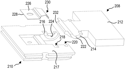
In the ever-evolving world of electronic devices, Microsoft Technology Licensing, LLC is looking to revolutionize the way we interact with our gadgets. With their newly patented hinge device, they aim to bring a seamless and flexible experience to electronic devices such as laptops, tablets, and smartphones. The hinge device consists of two parts that can move relative to each other, creating a versatile range of positions for the device. This movement is made possible by a biasing element, which is cleverly supported by either the first or second portion of the device. The first portion features an arcuate groove, while the second portion has an arcuate rail that smoothly slides within the groove. This complementary design allows for a sturdy yet adaptable connection between the two parts. What sets this hinge device apart is its bistability feature. In simpler terms, it means that the device can be locked in both closed and open states without the need for additional mechanisms. This is achieved through the clever application of radial force generated by the biasing element's unique surface profile, creating stability and ease of use. While this patent description sounds promising, it is important to note that not all patented ideas become actual products. Competitors such as Apple with their MacBo. ok lineup and Samsung with their Galaxy laptops have made significant strides in hinge technology. However, if Microsoft successfully brings this invention to market, it could find applications in a wide range of electronic devices, enhancing user experiences and setting a new standard for flexible design. As we eagerly await the future of this hinge device, one question arises: Could this technology be the game-changer that the industry has been waiting for? How would you envision making use of such a versatile hinge in your own electronic devices? Share your thoughts in the comments below.
The hinge device described in this patent allows for an electronic device to be supported by a biasing element that can move between two positions, a closed state and an open state. The biasing element contacts the leading edge of the other of the first portion or second portion, and depending on the position of the biasing element, these portions are bistable in either of these states. This allows for easy adjustment of the angle at which an electronic device is held, making it easier to use.
US Patent 11809238
Dell Products L. P.
Information Handling System Keeps processors and resources powered down to avoid overloading
What is this invention?
Systems and methods for itemizing device inventory for system power management
An information handling system with care,
A processor and resources to share,
Power subsystems are needed,
With limits that must be heeded,
Else remedial action will ensnare.
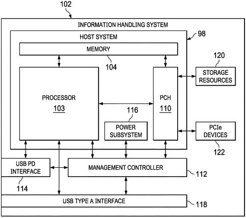
Dell Products L. P. has recently been granted a patent for an information handling system that aims to manage power consumption in a more efficient way. The system comprises a processor, multiple information handling resources, a power subsystem, and a management controller. The management controller plays a crucial role in this system, as it creates an inventory of all the information handling resources and determines the worst-case maximum power consumption of the processor and these resources. If this consumption exceeds the power limit associated with the power subsystem, the management controller takes remedial action to maintain the power usage below the limit. This patent highlights Dell's commitment to developing solutions that optimize power consumption and ensure efficient operation of their devices. While many may argue that such power management features already exist in competitor's products, Dell's approach seems to focus on accurately determining the worst-case maximum power consumption, allowing for proactive measures to be taken. Beyond traditional information handling devices, one can imagine potential applications for this technology in various sectors. For instance, in data centers, where power consumption management plays a critical role, this system could help maintain power limits and prevent overloads. Despite the potential usefulness of this patent, it's worth noting that not all patented technologies end up being incorporated into commercial products. Many factors come into play, including market demand, feasibility, and cost. So the question remains, how likely is it that Dell will turn this power management system into a tangible product? Let us know your thoughts in the comments below. Do you believe Dell's patent brings something unique to the table, or is it merely an incremental improvement on existing solutions?
An information handling system may include a processor, a plurality of information handling resources communicatively coupled to the processor, a power subsystem configured to deliver electrical energy to the processor and the plurality of information handling resources to enable operation of the processor and the plurality of information handling resources, and a management controller. The management controller may be configured to create an inventory of the plurality of information handling resources; based on the inventory, determine a worst-case maximum power consumption of the processor and the plurality of information handling resources; determine if the worst-case maximum power consumption exceeds a power limit associated with the power subsystem; and if the worst-case maximum power consumption exceeds the power limit, cause a remedial action to be taken to maintain power consumption of the processor and the plurality of information handling resources below the power limit.
US Patent 11809261
Dell Products L. P.
Telemetry data predicts imminent exothermic failure in IHS
What is this invention?
Exothermic failure prediction engine
A system was created to detect,
When exothermic failures were suspected.
The RAC collected data,
To determine the fate,
And prevent damage when detected.
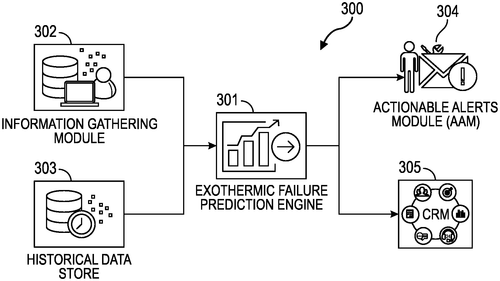
Dell has recently filed a patent that describes systems and methods for an "exothermic event prediction engine." In simple terms, this invention aims to prevent overheating and potential failure in its Information Handling Systems (IHS). By collecting telemetry data from the IHS and analyzing it, the Remote Access Controller (RAC) can predict when an exothermic failure may occur. While the potential applications of this technology are clear, the key question remains: will Dell actually turn this concept into a real product? Competitors like HP and Lenovo already offer sophisticated thermal management solutions for their devices, so Dell will need to carefully consider whether their exothermic event prediction engine is a viable addition to their lineup. If Dell were to bring this technology to market, it could undoubtedly find its place in critical infrastructure settings, data centers, or even high-performance gaming PCs where thermal management is crucial. However, the real-world practicality of such a system may be limited for everyday consumers who generally don't face exothermic failures in their personal devices. What are your thoughts on Dell's potential implementation of this exothermic event prediction engine? Do you believe it could truly revolutionize the industry, or is it simply another patent filing we may never see in action? Share your insights in the comments below.
The embodiments described herein provide systems and methods for predicting exothermic failures in an information handling system. In one embodiment, the RAC collects telemetry data from the IHS and predicts an exothermic failure in the IHS based, at least in part, upon the telemetry data. As such, embodiments of the invention can be used to prevent or reduce damage caused by exothermic failures in information handling systems.
US Patent 11809264
Dell Products L. P.
Storage Array Localizes Link Issues
What is this invention?
Discovering host-switch link and ISL issues from the storage array
There once was a detector so fine,
It monitored ports of the storage array line.
For IO failures and local link errors it did detect,
And determined if congestion was to be expected.
The flag indicated an issue with hosts or switches in sight,
So the detector could quickly identify what wasn't quite right!
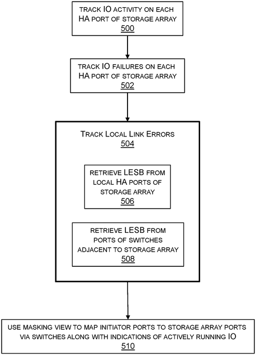
In a recent patent application by Dell Products L. P., a congestion and failure detector and localizer has been described. This innovative technology aims to address the common challenges faced in storage arrays, such as IO failures, local link errors, and congestion issues. The congestion and failure detector and localizer operates by locally monitoring the ports of the storage array for IO failures and local link errors. It also remotely monitors the ports of host initiators, as well as host-side and storage array-side switches for link errors. By analyzing various factors, including the increasing local link error rate, association of IO failures with a single host initiator port, and a rise in link error rate on both the host initiator and initiator-side switch, this detector can generate a flag that indicates the specific issue being faced. This patent application is an interesting development in the field of storage arrays and has the potential to greatly enhance the efficiency and performance of these systems. However, it is worth noting that a patent application does not necessarily guarantee the development of an actual product. Many factors, including market demand, competition, and feasibility, come into play when deciding whether an invention will make it to the market. If this technology were to be implemented, it could revolutionize the way storage arrays are managed and monitored. It could provide real-time insights into the root causes of congestion and failure, enabling faster troubleshooting and resolution. Additionally, it could help identify physical link problems, ISL physical issues, spreading congestion, host initiator-side physical link problems, and path congestion, providing valuable information to IT professionals. As we eagerly await further updates on the development of this invention, it would be interesting to hear your thoughts. How do you envision such a congestion and failure detector and localizer being utilized, and what potential benefits can you foresee? Share your insights in the comments below!
The text describes a congestion and failure detector and localizer that runs on a storage array. The detector monitors ports of the storage array for IO failures and local link errors, and generates a flag indicating either a physical link problem between the storage array and adjacent switch, ISL physical issue or spreading congestion, host initiator-side physical link problem, or path congestion. Based on this information, the detector determines whether there is an issue with the storage array's connections to adjacent switches or hosts.
US Patent 11809268
Dell Products L. P.
Manage data processing systems with anomalous behavior detection
What is this invention?
System and method for identifying anomalies in data logs using context-based analysis
A data processing system manager,
Was tasked with a tricky endeavor.
Logs were obtained to identify state,
Inference models implemented to anticipate,
To reduce the risk of becoming impaired!
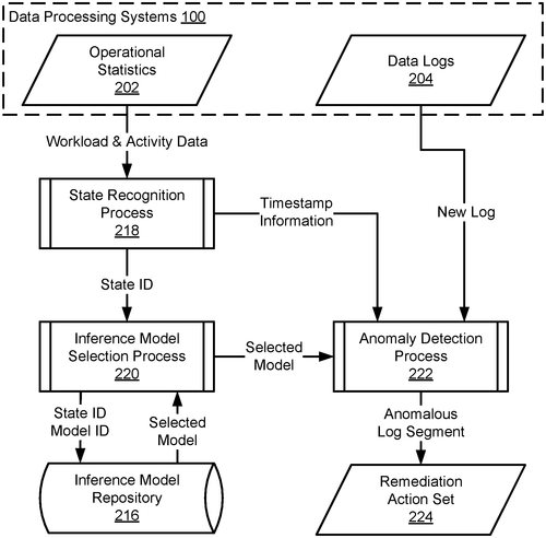
Dell Products L. P. has recently filed a patent that explores methods and systems for managing data processing systems based on indications of anomalous behaviors in logs. This innovation aims to improve the operational efficiency and reliability of data processing systems by using historical and current log information to predict future infrastructure issues. The core concept behind this patent is to allow a data processing system manager to obtain logs that provide insights into the operation of various hardware and software components. By analyzing these logs, the manager can identify the current operational state of the system, which enhances the context of the log information for more accurate predictions. The innovation lies in the implementation of inference models that can detect anomalous behaviors recorded in the logs. These models predict future infrastructure problems, helping the data processing system manager take proactive measures to reduce the likelihood of system impairment. While this patent showcases a promising approach to data processing system management, it is important to note that the filing of a patent does not necessarily imply that it will result in a commercial product. Competitor products, such as IBM's Watson AIOps or Splunk's IT Service Intelligence, have already made strides in similar areas, offering monitoring and predictive analytics for data processing systems. Looking forward, one can imagine potential applications for this technology in various industries where data processing systems are critical. For example, it could be employed in healthcare settings to ensure the continuous and efficient operation of electronic health record systems, or in financial institutions to improve the reliability of transaction processing systems. As we explore the possibilities presented by this patent, it is essential to consider how this innovation could impact organizations dealing with large-scale data processing systems. How crucial do you think proactive system management is to ensure uninterrupted operations in today's data-centric world? Share your thoughts in the comments below.
A data processing system may include and depend on the operation of hardware and/or software components. To manage the operation of the data processing system, a data processing system manager may obtain logs for components of the data processing system that reflect the historical and/or current operation of these components. The logs may be used to identify the operational state of the data processing system, improving the context of log information. Based on identified state, inference models may be implemented to predict future infrastructure issues by detecting anomalous behaviors recorded in logs. Based on predictions, action may be taken to reduce likelihood of data processing system becoming impaired.
US Patent 11809271
Dell Products L. P.
Embodiments of Systems and Methods for High-Availability (HA) Management Networks for High Performance Computing (HPC) Platforms
What is this invention?
High-availability (HA) management networks for high performance computing platforms
A system for HPC platforms was made
That High Availability could be displayed
The first BMC had a port
But the second one fell short
So both shared to ensure it stayed grade A
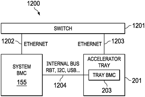
Dell Products L. P. has recently filed a patent for systems and methods aimed at enhancing the high-availability (HA) management networks of High Performance Computing (HPC) platforms. The proposed solution involves incorporating a first Baseboard Management Controller (BMC) with a first network port, along with a hardware accelerator housing a second BMC equipped with a second network port. The innovation lies in the ability of these controllers to dynamically share network ports in response to failure or insufficient bandwidth. In the competitive realm of HPC platforms, where speed and reliability are of utmost importance, Dell's patent appears to offer a potential edge. By enabling the BMCs to share network ports when necessary, this solution ensures uninterrupted communication within the system, even in the face of connectivity issues. This feature brings the promise of improved availability and performance to HPC platforms, benefiting industries relying on these high-performance computing systems, including scientific research, weather modeling, and financial services. While the patent holds promise, it's important to note that not all patents translate into commercial products. Dell will ultimately need to assess the feasibility, demand, and potential scalability of this technology before it becomes a reality. Additionally, competitors in the HPC market might already be working on similar solutions or could offer alternative products with similar capabilities. Nevertheless, if implemented successfully in future HPC platforms, Dell's invention could revolutionize the way high-availability management networks are established. The versatility offered by the dynamic sharing of network ports has the potential to optimize performance and maintain uptime, making this technology worth keeping an eye on in the HPC arena. What potential applications do you envision for this high-availability management network technology? How do you think it will impact the performance and reliability of HPC platforms? Share your thoughts in the comments below.
Embodiments of systems and methods for high-availability (HA) management networks for High Performance Computing (HPC) platforms are described. In some embodiments, an HPC platform may include a first Baseboard Management Controller (BMC) having a first network port; and a hardware accelerator comprising a second BMC having a second network port, where at least one of: (a) the first BMC is configured to share the first network port with the second BMC in response to a determination that the second network port has failed or has insufficient bandwidth, or (b) the second BMC is configured to share the second network port with the first BMC in response to a determination that the first network port has failed or has insufficient bandwidth.
US Patent 11809289
Intel Corporation
Access to Daughter Die Logic Controlled Via Arbitrator
What is this invention?
Apparatus and method for reusing manufacturing content across multi-chip packages
A daughter die and an arbitrator,
Connected to a testing device greater.
The enable logic will hear,
What message the main die does steer.
Then control is given for access much later!
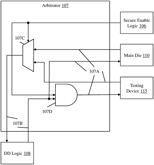
Intel Corporation has recently been granted a patent for an intriguing apparatus that could revolutionize the testing process for multi-chip packages (MCPs). The patent describes an apparatus composed of a daughter die logic (DD), an arbitrator, an external testing device, and a main die (MD). The key feature of this invention is the enable logic, which is designed to receive messages from the MD. Based on these messages, the enable logic determines whether the MD or the external testing device should have access to the DD logic. If the external testing device is deemed enabled, the arbitrator is then controlled to grant it access to the DD logic. While the patent's description does not explicitly refer to any competitor's products, it is clear that Intel aims to address the challenges and limitations associated with testing MCPs. Traditional testing methods often require complex setups and intricate circuitry, making the process time-consuming and resource-intensive. By introducing an apparatus that facilitates efficient testing and grants external devices access to the DD logic, Intel could potentially streamline the testing process for MCPs, leading to increased productivity and cost savings for manufacturers. Imagine the possibilities! This invention could accelerate the development and testing of new MCPs, allowing for rapid iterations and innovations in the field. It could also pave the way for more advanced quality control techniques, ensuring that MCPs meet the highest standards before reaching the market. However, it is important to approach this patent with a hint of skepticism. Being granted a patent is a significant milestone, but it does not guarantee that the described invention will become a viable product. Numerous patents remain unrealized, either due to technical challenges, market viability concerns, or other external factors. The true impact of Intel's apparatus will ultimately depend on its successful implementation, integration into existing systems, and market demand. What are your thoughts on Intel's patent? Can you envision any specific applications for this apparatus in the semiconductor industry or beyond? Share your insights and opinions in the comments section below!
The apparatus includes a daughter die (DD) logic, and an arbitrator connected to the DD logic, and connected to an external testing device and a main die (MD) included in a multi-chip package (MCP). The enable logic is configured to receive a message from the MD, based on the received message, determine whether the MD or the external testing device is enabled to access the DD logic. If it is determined that the MD is enabled to access the DD logic, then control is given to the arbitrator to enable the external testing device to access the DD logic.
US Patent 11808811
Intel Corporation
Automatic Test Equipment Controlled to Keep DUT Junction Temperature at Pre-Determined Test Level
What is this invention?
Apparatus and method for controlling unit specific junction temperature with high temporal resolution for concurrent central processing unit (CPU) core testing
A processor to control the ATE
Measured parameters of a test instance, see?
It determined one or more
Controls for head's temperature floor
To make sure that DUT junction temp was key
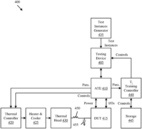
In a recent patent filing, Intel Corporation has introduced an apparatus that aims to revolutionize the testing process for devices under examination. This new invention involves a processor that controls an automatic test equipment (ATE) to measure various parameters during the execution of a current test instance on the device under test (DUT). Based on these measurements, the processor determines precise controls for regulating the temperature of a thermal head connected to the DUT. The end goal is to ensure that the junction temperature of the DUT corresponds to a predetermined test temperature. While the patent does not provide specific details on the mechanics of the apparatus, it presents a promising development that could significantly enhance the accuracy and efficiency of testing procedures. By precisely controlling the thermal conditions during testing, the device's performance under real-world circumstances can be better evaluated. Currently, the market offers limited alternatives to this proposed invention. Competitors typically rely on manual adjustments or imprecise settings to regulate the temperature during testing. However, Intel's apparatus offers a more systematic and data-driven approach that could outperform existing solutions. The potential applications of this technology are vast. Manufacturers of electronic devices, ranging from microprocessors to integrated circuits, could benefit from improved testing accuracy. By ensuring that devices comply with predetermined performance thresholds, this innovation has the potential to enhance the overall quality and reliability of products. Nevertheless, it is important to note that just because a patent is filed does not guarantee that the technology will be implemented as a final product. Many factors, such as feasibility, market demand, and cost considerations, come into play during the development process. Considering the significance of this patent, readers are invited to share their thoughts on the potential impact of Intel's invention. Do you believe this apparatus has the potential to redefine the testing landscape for electronic devices? Feel free to leave your comments below.
The apparatus includes a processor that controls an automatic test equipment (ATE) to measure one or more parameters of a current test instance for testing a device under test (DUT). The processor determines, based on the measured one or more parameters, one or more controls for controlling a temperature of a thermal head connected to the DUT so that the junction temperature of the DUT corresponds to the predetermined test temperature.
US Patent 11808813
Intel Corporation
Capture Die Fiducial Images with the Same Precision Every Time
What is this invention?
Method and device for fast, passive alignment in photonics assembly
A die with a cavity so deep,
Was fitted with a lens to keep.
The image was caught
When the fiducials were sought,
Until they both seemed to meet in one leap!
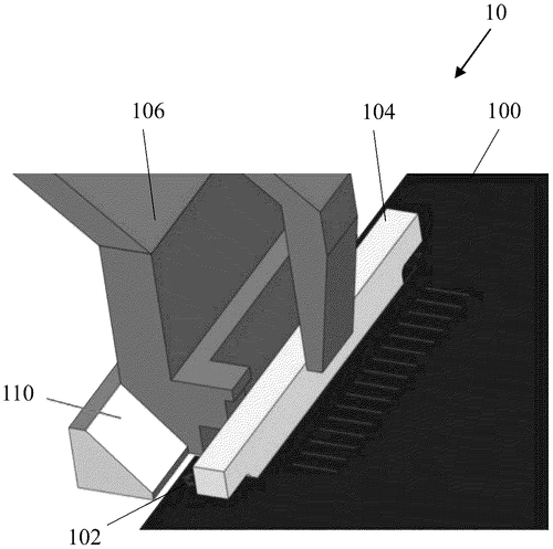
Intel Corporation has recently filed a patent that introduces a novel method for capturing accurate images using lens structures within a die. The patent describes a process whereby a cavity is created within the die, which includes fiducials on both the die's top surface and the front surface of the lens structure. By aligning these fiducials and positioning the lens structure within the cavity, an image processing system can capture clear images when the fiducials coincide and lie in a plane perpendicular to the die's top surface. Although the patent provides an intriguing concept for enhancing image quality, it is important to note that patents do not always result in commercially available products. Intel's inventive approach potentially introduces new possibilities for image capture and processing, but it remains to be seen whether the company will pursue the development and production of such a system. In a market flooded with various imaging technologies, Intel would face competition from established players such as Canon, Nikon, and Sony, who consistently strive to improve their cameras' capabilities. However, Intel's unique integration of lenses within a die could lead to innovations in compact devices like smartphones and tablets, where space is limited. The potential use cases for this technology are diverse. For example, it could enable smaller, more powerful cameras in wearable devices, allowing for better image quality and enhanced user experiences. In medical imaging, this method might find applications in endoscopy or other minimally invasive procedures where clear, high-quality images are essential. Intel's patent raises interesting questions about the future of imaging technologies. How important is image quality to you in the devices you use on a daily basis? Are there specific areas of your life or work where improved image capture capabilities would significantly benefit you? Share your thoughts and ideas in the comments below.
The present disclosure relates to a method including providing a die including a cavity therein, wherein the die further may include a die fiducial on a top surface. The method further includes placing a lens structure in the cavity of the die, wherein the lens structure may include a lens fiducial on a front surface. The method also includes moving the lens structure in the cavity to a position until an image processing system captures an image of the lens fiducial and die fiducial that coincide and lie in a plane orthogonal to top surface of the die.
US Patent 11808988
Intel Corporation
Electronic Device with Custom Hinge Angle
What is this invention?
Hinge angle detection
A device with two housings, a hinge did connect;
It measured the angle using data to detect.
The accelerometers and gyroscopes would check,
To see if in motion or portrait it'd be set.
If not in either one of these states, you could expect!
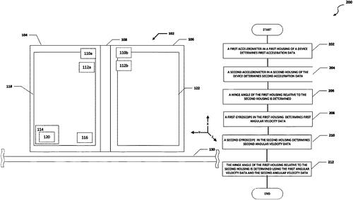
Intel Corporation has recently filed a patent for an intriguing electronic device that could revolutionize the way we interact with our gadgets. The patent describes a device with two housings joined together by a hinge, each housing equipped with accelerometers and gyroscopes. What makes this invention interesting is its ability to determine the angle of the hinge based on the data collected by these sensors. When the device is not in motion or in a portrait orientation, the angle is calculated using the accelerometers and gyroscopes from both housings. However, if the device is in motion or in a portrait orientation, the angle is determined solely by the gyroscopes. While the patent doesn't specifically mention what type of device this could be, one can imagine a variety of potential applications. For instance, such technology could find its way into the next generation of smartphones or tablets, allowing for smoother transitions between portrait and landscape orientations. It could also enhance the functionality of foldable devices, ensuring a seamless experience as users open and close their gadgets. Competitors like Samsung and Motorola have already released foldable smartphones, but none of them have incorporated this level of hinge-angle detection into their designs. If Intel brings this invention to market, it could give them a competitive edge in the rapidly evolving world of handheld devices. However, it's important to note that patents do not always translate into actual products. Many patents are filed purely for defensive purposes or to protect intellectual property. So, while this invention certainly has potential, we'll have to wait and see if Intel decides to turn it into a consumer product. What are your thoughts on this patent? Do you see yourself benefiting from a device with such hinge-angle detection capabilities? Let us know in the comments below!
An electronic device includes a first housing, a second housing, and a hinge. The hinge rotatably couples the first housing to the second housing. A hinge angle is determined using data from the first housing accelerometer, the second housing accelerometer, the first house gyroscope, and the second house gyroscope if the electronic device is not in motion or is in portrait orientation.
US Patent 11809237
Intel Corporation
Power-Constrained Computers Can Be Improved By Learning How To Run At Maximum Frequency
What is this invention?
Workload aware power limiting and multiple-input multiple-output control
A scheme of great complexity
Can improve the performance, we see
It learns coefficients fast
To ensure power won't be surpassed
And maximizes each compute element's frequency
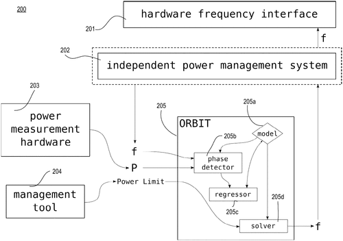
Intel Corporation has recently patented a scheme that aims to improve the performance of power-constrained computers. This scheme involves a heterogeneous mix of compute elements, which dynamically react to changes in switching capacitance induced by the workload. By learning the coefficients of a power-frequency model for each compute element and forecasting the maximum frequency at each time step, the scheme ensures that the compute elements operate at their maximum frequency without exceeding the input power limit. Power-constrained computers have always been a challenge, as increasing performance often comes at the cost of more power consumption. This patent by Intel attempts to tackle this issue by efficiently managing the power-frequency relationship in a heterogeneous compute environment. Heterogeneous computing, which involves combining different types of compute elements, is not a novel concept. Competitors like AMD and Nvidia have been exploring this field with their integrated graphics processing units (GPUs) and CPUs, which offer improved performance and energy efficiency. However, Intel's scheme takes a different approach by dynamically adjusting the frequency of compute elements to maximize performance without exceeding power limits. Imagine the potential uses of this technology in mobile devices, where the power constraints are even more critical. By optimizing the power consumption and performance of individual compute elements, Intel's scheme could lead to longer battery life without compromising on computing power. While the concept behind Intel's patent seems promising, it's important to remember that not all patented inventions translate into marketable products. The field of technology is brimming with exciting ideas, but practicality and feasibility play a significant role in determining whether these ideas will come to fruition. What are your thoughts on Intel's novel power-frequency scheme for power-constrained computers? Can you envision any other potential applications for this technology? Share your insights in the comments below.
This paper describes a scheme that can improve performance of power-constrained computers by dynamically reacting to changes in the switching capacitance that present workload induces in each heterogeneous compute element and learning the coefficients of a power-frequency model for each compute element. At each time step, the scheme forecasts a maximum frequency that the compute element can run at without exceeding an input power limit for a given workload. The scheme rapidly re-learns coefficients of the power model and rapidly adapts the frequency as the workload's characteristics shift ensuring that compute elements run at the maximum frequency they can while not exceeding the input power limit.
US Patent 11809250